
Abstract
Deposition of thin-films used in MEMS and NEMS devices rely on a wide variety of technologies. Physical vapor deposition (PVD) uses physical effects like evaporation or ion bombardment to create thin-films on a substrate by forcing source atoms into a gaseous phase. Chemical vapor deposition (CVD) and similar processes create coatings by a chemical reaction of volatile species by using reaction processes defined by chemical reaction equations. While PVD and CVD are dry processes, for depositing conductive thin-films the substrate may be submerged in an electrically conductive liquid (an electrolyte) and subjected to electrochemical or chemical deposition. Spin-coating and spray-coating are two examples of technologies that lend themselves to creating organic films—a technology widely used in depositing photoresists in photolithography. Dip processes like solgel may be used for the creation of oxide coatings.
Access this chapter
Tax calculation will be finalised at checkout
Purchases are for personal use only
Notes
- 1.
Heinrich Hertz was a brilliant scientist who passed away at the age of only 37. He is most famous for providing experimental proof for Maxwell’s Laws and converting Maxwell’s equations into a more practical form [20].
- 2.
An electron volt (eV) is the amount of energy an electron gains when traveling through an electric potential of one volt. 1 electron volt = 1.6 × 10⁻¹⁹ joule [1].
- 3.
English pronunciation: deh-BYE (rhymes with cry).
- 4.
For more information about HARMST , see Chap. 7.
References
Ohring M (2002) Material science of thin films, deposition and structure, 2nd edn. Academic Press, San Diego
Gad-el-Hak M (ed) (2006) The MEMS handbook, 2nd edn. CRC Press, Boca Raton
Goddard WA III, Brenner DW, Lyshevski SE, Iafrate GJ (eds) (2007) Handbook of nanoscience, engineering, and technology. CRC Press, Boca Raton
Madou M (2011) Fundamentals of microfabrication and nanotechnology, 3rd edn. CRC Press, Boca Raton
Martin PM (2010) Deposition technologies: an overview. In: Martin PM (ed) Handbook of deposition technologies for films and coatings, 3rd edn. Elsevier, Oxford
Vossen JL, Kern W (eds) (1991) Thin film processes II. Academic Press, San Diego
Deshpandey C, Bunshah P (1991) Evaporation processes. In: Vossen JL, Kern W (eds) Thin film processes II. Academic Press, San Diego
Shah SI, Jaffari GH, Yassitepe E, Ali B (2010) Evaporation: processes, bulk microstructures, and mechanical properties. In: Martin PM (ed) Handbook of deposition technologies for films and coatings, 3rd edn. Elsevier, Oxford
Parsons R (1991) Sputter deposition process. In: Vossen JL, Kern W (eds) Thin film processes II. Academic Press, San Diego
Depla D, Mahieu S, Greene JE (2010) Sputter deposition processes. In: Martin PM (ed) Handbook of deposition technologies for films and coatings, 3rd edn. Elsevier, Oxford
Jensen KF, Kern W (1991) Thermal chemical vapor deposition. In: Vossen JL, Kern W (eds) Thin film processes II. Academic Press, San Diego
Reif R, Kern W (1991) Plasma-enhanced chemical vapor deposition. In: Vossen JL, Kern W (eds) Thin film processes II. Academic Press, San Diego
Carlsson J-O, Martin PM (2010) Chemical vapor deposition. In: Martin PM (ed) Handbook of deposition technologies for films and coatings, 3rd edn. Elsevier, Oxford
Martinu L, Zabeida O, Klemberg-Sapieha JE (2010) Plasma-enhanced chemical vapor deposition of functional coatings. In: Martin PM (ed) Handbook of deposition technologies for films and coatings, 3rd edn. Elsevier, Oxford
Lowenheim FA (1978) Deposition of inorganic films from solutions. In: Vossen JL, Kern W (eds) Thin film processes. Academic Press, New York
Thompson LF, Willson CG, Bowden MJ (eds) (1994) Introduction to microlithography, 2nd edn. American Chemical Society, Washington
Klein LC (1991) Sol–gel coatings. In: Vossen JL, Kern W (eds) Thin film processes. Academic Press, New York
Faraday M (2013) BBC History. http://www.bbc.co.uk/history/historic_figures/faraday_michael.shtml. Accessed 02 Feb 2013
Faraday Michael (1857) The Bakerian Lecture: Experimental relations of gold (and other metals) to light. Phil Trans R Soc Lond 147:145–181. doi:10.1098/rstl.1857.0011
Lederman L (2006) The god particle: if the universe is the answer, what is the question?. Houghton Mifflin, New York
Eckert M (2010) Heinrich Hertz. Ellert & Richter, Hamburg
Nahrwold R (1887) Ueber Luftelectricität (About air electricity). Ann Phys 267:448–473. doi:10.1002/andp.18872670708
Kundt A (1888) Über die Brechungsexponenten der Metalle (About refractive indices of metals). Ann Physik 34:469–489. doi:10.1002/andp.18882700705
Myoptica: Zeiss T (2012) Anti-reflective Coatings. http://www.myoptica.com/helpar.cfm. Accessed 27 July 2012
Clausius R (2012). http://www.nndb.com/people/951/000100651/. Accessed 12 Dec 2012
Benoit Paul Émile Clapeyron (1998) http://www-history.mcs.st-andrews.ac.uk/Biographies/Clapeyron.html. Accessed 12 December 2012
van ′t Hoff JH (1902) Raoult Memorial Lecture. J Chem Soc Trans 81:969–981. doi:10.1039/CT9028100969
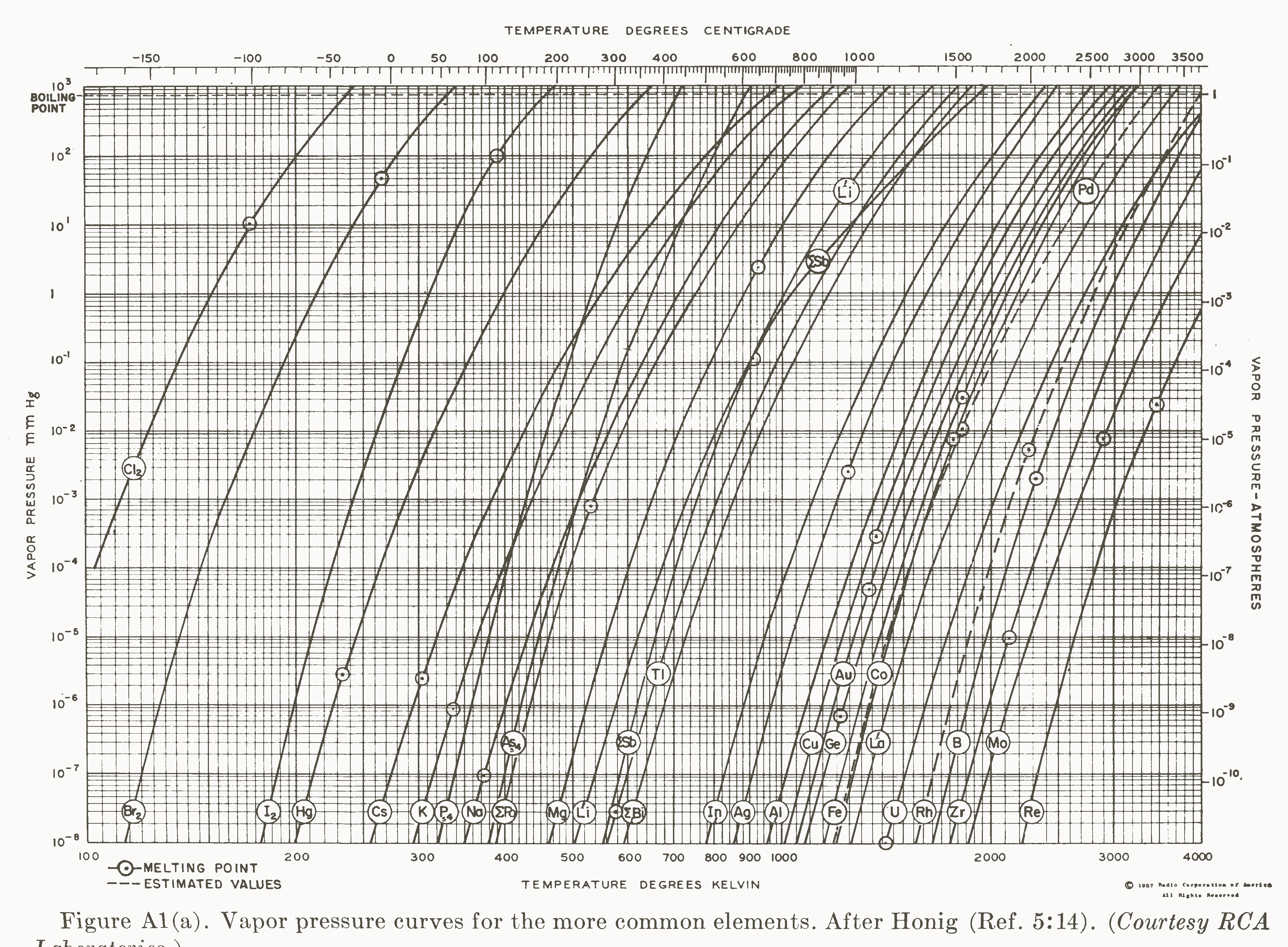
Honig RE (1957) Water pressure data for the more common elements. David Sarnoff Research Center, Princeton NJ, USA 1957, http://www.powerstream.com/z/vapor-press2-big.png. Accessed 21 Sept 2012
Christensen TM (2000) Physics of thin films (lecture notes). http://www.uccs.edu/~tchriste/courses/PHYS549/549lectures/evap.html. Accessed 12 Dec 2012
RD Mathis Company (2012) Product information. http://www.rdmathis.com/prodinfo.htm. Accessed 12 Dec 2012
Roberts Jr GC, Via GG (1967) Monitored evaporation. US patent 3,313,914
Standard Electron Beam Evaporator (2014) Dr. Eberl MBE Komponenten, Weil der Stadt, Germany
Optics Balzers (2012) Enabling innovative optical solutions. http://www.opticsbalzers.com/download_temp/oba_imagebroschuere_low.pdf. Accessed 06 Dec 2012
Chow PP (1991) Molecular beam epitaxy. In: Vossen JL, Kern W (eds) Thin film processes II. Academic Press, San Diego
Biasiol G, Sorba L (2001) Molecular beam epitaxy: principles and applications. In: Fornari R, Sorba L (eds) Crystal growth of materials for energy production and energy-saving applications. Edizioni ETS, Pisa, Italy
Kern W, Bahn VS (1978) Chemical vapor deposition of inorganic films. In: Vossen JL, Kern W (eds) Thin film processes. Academic Press, New York
Adam H, Steckelmacher W (1994) Martin Knudsen. In: Redhead PA (ed) Vacuum science and technology: Pioneers of the 20th century. History of vacuum science and technology, vol 2. AIP Press, New York
Barron AR (2014) Molecular beam epitaxy. http://cnx.org/content/m25712/latest/. Accessed 26 March 2014
Kreutz EW (1998) Pulsed laser deposition of ceramics—fundamentals and applications. Appl Surf Sci 127–129:606–613. doi:10.1016/S0169-4332(98)00107-X
Andor Technology (2012) Pulsed laser deposition. http://www.andor.com/learning-academy/pulsed-laser-deposition-an-introduction-to-pulsed-laser-deposition. Accessed 12 December 2012
PLD Plume (2014) Wikimedia commons. http://en.wikipedia.org/wiki/File:PLD_Plume.png. Accessed 26 March 2014
Naval Research Lab Technology Transfer Office (2012) Pulsed laser deposition of ceramics. http://www.nrl.navy.mil/techtransfer/fs.php?fs_id=MAT19. Accessed 15 Dec 2012
Anders A (2010) Unfiltered and filtered cathodic arc deposition. In: Martin PM (ed) Handbook of deposition technologies for films and coatings, 3rd edn. Elsevier, Oxford
Kinston E (2008) Joseph Priestley (1733–1804). Internet Encycl Philosophy. http://www.iep.utm.edu/priestly/. Accessed 15 Dec 2012
Priestley J (1775) Experiments in which rings, consisting of all the prismatic colours, were made by electrical explosions on the surface of metals. In: The history and present state of electricity, vol II. London, pp 329–335
McEvoy JG (2013) Joseph Priestly. Encycl Britannica. http://www.britannica.com/EBchecked/topic/475975/Joseph-Priestly. Accessed 18 Jan 2013
Boxman RL (2001) Early history of vacuum arc deposition. IEEE Trans Plasma Sci 29:759–761
Wright AW (1877) On the production of transparent metallic films by the electrical discharge in exhausted tubes. Am J Sci Arts 13:49–55
Thomas Alva Edison Biography (2012) Rutgers. http://edison.rutgers.edu/biogrphy.htm. Accessed 26 March 2014
Edison TA (1892) Process of duplicating phonograms. US patent 484 582
Mattox DM (2003) The foundations of vacuum technology. Springer, Heidelberg
Sir William Grove (1811–1896). http://www.corrosion-doctors.org/Biographies/GroveBio.htm. Accessed 15 Dec 2012
Grove WR (1852) On the electrochemical polarity of gases. Phil Trans Roy Soc (Lond) B 142, p 87
Hinshelwood CN (1927) William Crookes, a Victorian man of science. http://www.chem.ox.ac.uk/icl/heyes/LanthAct/Biogs/Crookes.html. Accessed 15 Dec 2012
Irving Langmuir—Biography (2012). Nobelprize.org. Nobel Media AB. http://www.nobelprize.org/nobel_prizes/chemistry/laureates/1932/langmuir-bio.html. Accessed 15 Dec 2012
Plasma Physics–History. http://www-spof.gsfc.nasa.gov/Education/whplasma.html. Accessed 15 Dec 2012
Langmuir I (1929) The interaction of electron and positive ion space charges in cathode sheaths. Phys Rev 33:954–989
Rossnagel SM (1991) Glow discharge plasmas and sources for etching and deposition. In: Vossen JL, Kern W (eds) Thin film processes II. Academic Press, San Diego
Bogaerts A, Neyts E, Gijbels R, van der Mullen J (2002) Gas discharge plasmas and their applications (review). Spectrochimica Acta Part B 57:609–658
Townsend, Sir John Searly Edward. Oxford Dictionary of National Biography. http://www.oxforddnb.com/view/printable/36541. Accessed 15 Dec 2012
Paschen, Louis Carl Heinrich Friedrich (2008) Encyclopedia.com. http://www.encyclopedia.com/doc/1G2-2830903302.html. Accessed 28 March 2014
Glow Discharges (2014) Glow discharge laboratory. http://www.glow-discharge.com/?Physical_background:Glow_Discharges. Accessed 28 March 2014
NASA Science (2001) Definition of an electron volt. http://science.nasa.gov/science-news/science-at-nasa/2001/comment2_ast15jan_1/. Accessed 15 Dec 2012
Peter Debye—Biographical (1966) Nobelprize.org. Nobel Media AB. http://www.nobelprize.org/nobel_prizes/chemistry/laureates/1936/debye-bio.html. Accessed 28 March 2014
Sigmund P (1969) Theory of sputtering. I. Sputtering yield of amorphous and polycrystalline targets. Phys Rev 184:383–416
Ginsburg E (2002) Sputtering. Intel. www.eng.tau.ac.il/~yosish/courses/vlsi/Sputtering1.ppt. Accessed 03 Dec 2012
Maidhof H (1980) General information on the cathodic sputtering process. Application note, Leybold Heraeus, now Oerlikon Leybold Vacuum, Cologne, Germany
Small Sputtering. Application note. Leybold Heraeus, now Oerlikon Leybold Vacuum, Cologne, Germany
Sputtering Specifications. Mycralyn MEMS Foundry, Edmonton, AB (Canada). http://www.micralyne.com/thin-film-sputtering/. Accessed 15 Dec 2012
Colligon JS (2004) Ion-assisted sputter deposition (review). Phil Trans R Soc Lond A 362:103–116. doi:10.1098/rsta.2003.1303
Johnson PC (1991) The cathodic arc deposition of thin films. In: Vossen JL, Kern W (eds) Thin film processes II. Academic Press, San Diego
Takikawa H, Tanoue H (2007) Review of cathodic arc deposition for preparing droplet-free thin films. IEEE Trans Plasm Sci 35:992–999
Martin PM (2012) Guides to vacuum processing: filtered cathodic arc deposition. http://www.jh-vac.com/image/pdf/filtered%20cathodic%20arc%20deposition.pdf. Accessed 6 Dec 2012
Aksenov quarter torus filter (2012) Wikimedia Commons. http://en.wikipedia.org/wiki/File:AksenovQuaterTorusFilter.jpg. Accessed 15 Dec 2012
Bogy DB, Yun X, Knapp BJ (1994) Enhancement of head-disc interface durability by using diamond-like carbon overcoats on the sliders’ rails. IEEE Trans Magn 2:369–374
Anders A, Fong W, Kulkarni A, Francis W, Ryan FW, Bhatia CS (2001) Ultrathin diamond-like carbon films deposited by filtered carbon vacuum arcs. IEEE Plasm Sci 5:1–25
DLC Coatings, Diamonex DLC, Allentown PA. http://www.diamonex.com/products/dlc-coatings/?gclid=CJmHsfmznbQCFdG6zAod000ABQ. Accessed 15 Dec 2012
Allendorf M (1998) From Bunsen to VLSI—150 years of growth in chemical vapor deposition. Electrochem Soc Interface (Springer) 1998:1–3
Industrial Carbon. http://www.most.gov.mm/techuni/media/ChT_06014_16.pdf. Accessed 06 Dec 2012
Pakkala A, Putkonen M (2010) Atomic layer deposition. In: Martin PM (ed) Handbook of deposition technologies for films and coatings, 3rd edn. Elsevier, Oxford
Kern W, Ban VS (1978) Chemical vapor deposition of inorganic thin films. In: Vossen JL, Kern W (eds) Thin film processes. Academic Press, New York
Mond L, Langer C, Quincke F (1890) Action of carbon monoxide on nickel. J Chem Soc Trans 57:749–753. doi:10.1039/CT8905700749
Editors Encycl Britannica (2013) Ludwig Mond. Encycl Britannica. http://www.britannica.com/EBchecked/topic/389055/Ludwig-Mond. Accessed 18 Jan 2013
Crowther JG (2012) J Willard Gibbs. Encycl Britannica. http://www.britannica.com/EBchecked/topic/233207/J-Willard-Gibbs. Accessed 29 March 2014
Editors Encycl Britannica (2014) Enthalpy. Encycl Britannica. http://www.britannica.com/EBchecked/topic/188914/enthalpy. 29 March 2014
Drake GWF (2014) Entropy. Encycl Britannica. http://www.britannica.com/EBchecked/topic/189035/entropy. Accessed 29 March 2014
Sirtl E, Hunt LP, Sawyer DH (1974) High temperature reactions in the silicon–hydrogen–chlorine system. J Electrochem Soc 121:919–925
Ellingham diagrams (2013) MIT, Cambridge, MA. http://web.mit.edu/2.813/www/readings/Ellingham_diagrams.pdf. Accessed 19 Jan 2013
Ellingham Harald Johann Thomas (2013) AIM25 http://www.aim25.ac.uk/cgi-bin/vcdf/detail?coll_id=2625&inst_id=3&nv1=search&nv2=. Accessed 19 January 2013
Adolf Eugen Fick (1852–1937) Science museum. http://www.sciencemuseum.org.uk/broughttolife/people/adolfeugenfick.aspx. Accessed 14 Jan 2013
Rundle PC (1968) The epitaxial growth of silicon in vertical reactors. Int J Electronics 24:405–413
The Arrhenius Equation (2013) Shodor. http://www.shodor.org/unchem/advanced/kin/arrhenius.html. Accessed 17 Jan 2013
Svante Arrhenius—Biography (2013) Nobelprize.org. Nobel Media AB. http://www.nobelprize.org/nobel_prizes/chemistry/laureates/1903/arrhenius-bio.html. Accessed 17 January 2013
Kern W (1989) Chemical vapor deposition. In: Levy R, Levi RA (eds) Microelectronic materials and processes. Kluwer, Dordrecht
Sze SM, Ng KK (2006) Physics of semiconductor devices. Wiley, Hoboken
Ruska WS (1987) Microelectronic processing. McGraw-Hill, New York
Büttgenbach S (1994) Mikromechanik, 2nd edn. Teubner Studienbücher Angewandte Physik (Teubner textbooks of applied physics). B.G. Teubner, Stuttgart
Reinberg AR (1974) The hydrogen content of plasma-deposited silicon nitride. The Electrochem Soc Ext Abstr 74-1 # 6
Oxford Instruments (2013) Plasma enhanced chemical vapour deposition. http://www.oxford-instruments.com/products/etching-deposition-and-growth/plasma-etch-deposition/pecvd. Accessed 17 Jan 2013
Oxford Instruments (2013) Basic PECVD plasma processes (SiH based). www.ndl.narl.org.tw/cht/doc/3-1-1-0/T19/T19_B1.pdf. Accessed 17 Jan 2013
Mackencie KD, Johnson DJ, DeVre MW, Westerman RJ, Reelfs BH (2005) Stress control of Si-based PECVD dielectrics. In: 207th Electrochemical society meeting, proceedings of symposium silicon nitride and silicon dioxide thin insulating films and other emerging dielectrics VIII, PV2005-01, pp 148–159
Oxford Instruments (2013) Inductively coupled plasma chemical Vapour deposition (ICP CVD). http://www.oxford-instruments.com/products/etching-deposition-and-growth/plasma-etch-deposition/icp-cvd. Accessed 17 Jan 2013
Oxford Instruments (2013) ICP PECVD application note. http://www.oxfordplasma.de/technols/dpicpecr.htm. Accessed 23 Jan 2013
Oxford Instruments (2001) Application note PDT-06
Thomas O (2010) Inductively coupled plasma chemical vapour deposition (ICP-CVD)—White paper. Oxford Instruments Plasma Technology, Bristol
Roy SK (1988) Laser chemical vapour deposition. Bull Mater Sci 11:129–135
Eden JG (1991) Photochemical vapor deposition. In: Vossen JL, Kern W (eds) Thin film processes II. Academic Press, San Diego
Terrill RE, Church KH, Moon M (1998) Laser chemical vapor deposition for microelectronics production. IEEE Aerosp Conf 1:377–382
CVD Equipment Corporation (2013) Storage and gas delivery cabinets for UHP processes. http://www.products.cvdequipment.com/products/gascabinet/. Accessed 22 Jan 2013
CVD Equipment Corporation (2013) Exhaust gas conditioning system. http://www.products.cvdequipment.com/products/gascondsys/
Boyd SB (2012) Life cycle assessment of semiconductors. Springer, New York
Handbook Committee (1992) ASM Handbook, vol 10: materials characterization, 3rd printing. ASM International
Pinna N, Knez M (eds) (2012) Atomic Layer deposition of nanostructured materials. Wiley-VCH, Weinheim
Profijt HB, Potts SE, van de Sanden MCM, Kessels WMM (2011) Plasma-assisted atomic layer deposition: basics, opportunities, and challenges. J Vac Sci Technol A 29:050801. doi:10.1116/1.3609974
Puurunen RL (2005) Surface chemistry of atomic layer deposition: A case study for the trimethylaluminum/water process. J Appl Phys 97:121301. doi:10.1063/1.1940727
Suntola T (2004) Thirty years of ALD. http://www.sci.fi/~suntola/Presentations/2004%20HY,%2030%20years%20of%20ALD.pdf. Accessed 19 Jan 2013
Su JR (2012) Introduction to atomic layer deposition (ALD). National Chiao Tung University, Hsinchu, Taiwan. http://rdweb.adm.nctu.edu.tw/modules/mod_table/files/2011011710065875-4-0.pdf. Accessed 19 Jan 2013
Kessels E, Hodson Ch, Sharp T, Peter A (2012) Latest advances in plasma techniques for ALD. Oxford Instruments Plasma Technology, Bristol
Granneman E, Fischer P, Pierreux D, Terhorst H, Zagwijn P (2007) Batch ALD: Characteristics, comparison with single wafer ALD, and examples. Surf Coat Technol 201:8899–8907
Caro J (2013) Precursor composition. PCI, Leibniz Universität Hannover, Germany
Oxford Instruments (2013) Atomic layer deposition (ALD). http://www.oxford-instruments.com/products/etching-deposition-and-growth/plasma-etch-deposition/atomic-layer-deposition. Accessed 19 Jan 2013
Alasaarela T, Korn D, Alloatti L, Säynätjoki A, Tervonen A, Palmer R, J. Leuthold J, Freude W, Honkanen S (2011) Reduced propagation loss in silicon strip and slot waveguides coated by atomic layer deposition. Opt Express 19, 12:11529–11538. http://dx.doi.org/10.1364/OE.19.011529
Howson RP (1994) The reactive sputtering of oxides and nitrides. Pure Appl Chem 66:1311–1318
Hollars DR, Rosenblum MP, Peterson CT (2002) Sputtering apparatus and process for high rate coating. US patent 6,488.824. http://www.google.com/patents?hl=en&lr=&vid=USPAT6365010&id=s8MKAAAAEBAJ&oi=fnd&dq=Dual+Rotary+Magnetron+Coating&printsec=abstract#v=onepage&q=Dual%20Rotary%20Magnetron%20Coating&f=false. Accessed 5 Feb 2013
Olsson MK, Macák K, Graf W (1999) Reactive d.c. sputter deposited Al2O3 films: large-area coatings for industrial applications. Surf Coat Technol 122:202–207
Hollars DR (2001) Optical films by reactive sputtering. In: Proc 48th AVS international symposium, San Francisco
Thompson LF (1994) Resist processing. In: Thompson LF, Willson GC, Bowden MJ (eds) Introduction into microlithography, 2nd edn. American Chemical Society, Washington
MEMS Thin Film Deposition Processes (2013) MEMSnet®. http://www.memsnet.org/mems/processes/deposition.html. Accessed 02 Feb 2013
Spin Coating Theory (2013) IEEE components, packaging and manufacturing technology society. http://www.cpmt.org/mm/pkglab/theory/spin_theory.html. Accessed 02 Feb 2013
Paik J-A, Fan S-K, Chang H, Kim Ch-J, Wu MC, Dunn B (2004) Development of spin coated mesoporous oxide films for MEMS Structures. J Electroceram 13:423–428
Cooper KA, Hamel C, Whitney B (2007) Conformal photoresist coating for high aspect ratio features. In: Proceedings of the IWLPC. http://www.suss.com/fileadmin/user_upload/technical_publications/WP_Conformal_Photoresist_Coatings_for_High_Aspect_Ratio_Features_09.pdf. Accessed 02 Feb 2013
Süss MicroTec (2013) Enabling GYRSET coating technology. http://www.suss.com/en/products-solutions/products/spin-spray-coater-developer/options/enabling-gyrset-coating-technology.html. Accessed 04 Feb 2013
Pham NP, Boellard E, Sarro PM, Burghartz JN (2002) Spin, spray coating and electrodeposition of photoresist for MEMS structures—a comparison. Proc SAFE 2002, pp 81–85
Pham NP, Scholtes TL, Klerk R, Wieder B, Sarro PM, Burghartz JN (2001) Direct spray coating of photoresist for MEMS applications. doi:10.1117/12.442960
Pham NP, Burghartz JN, Sarro PM (2005) Spray coating of photoresist for pattern transfer on high topography surfaces. J Micromech Microeng 15:691–697
Pabo EF, Kurotaki H, Lindner P, Matthias T, Kettner P (2011) Advances in spray coating technologies for MEMS, 3DICs and additional applications. In: Proceeding of the IEEE 13th EPTC, pp 349–353
Dip Coating (2013) YTC America Inc. http://www.ytca.com/dip_coating. Accessed 6 Feb 2013
Satcher J (2005) Novel materials for chemistry. Sci Technol Rev 5. https://www.llnl.gov/str/May05/Satcher.html. Accessed 6 Feb 2013
Caro J (2013) PCI. Leibniz Universität Hannover, Germany
Schlesinger M, Paunovic M (eds) (2010) Modern Electroplating. Wiley, Hoboken
Ritzdorf T (2009) Electrochemical deposition processes and tools. In: Shacham-Diamand Y, Osaka T, Datta M, Ohba T (eds) Advanced nanoscale ULSI interconnects: fundamentals and applications. Springer, New York
The Baghdad Batteries (2013) Ancient Wisdom. http://www.ancient-wisdom.co.uk/baghdadbatteries.htm. Accessed 02 Feb 2013
National Museum Baghdad: 10 years later (2013) Archeology. http://www.archaeology.org/exclusives/articles/779-national-museum-baghdad-looting-iraq. Accessed 1 April 2014
Shukla AK, Kumar TP (2008) Pillars of modern electrochemistry: a brief history. Electrochem Encycl. http://electrochem.cwru.edu/encycl/art-p05-pillars-of-ec.htm. Accessed 2 Feb 2013
Schlesinger M (2013) Electroplating. Electrochem Encycl. http://electrochem.cwru.edu/encycl/art-e01-electroplat.htm, Accessed 14 Feb 2013
Editors Encycl Britannica (2013) Faraday’s laws of electrolysis. Encycl Britannica. http://www.britannica.com/EBchecked/topic/201755/Faradays-laws-of-electrolysis. Accessed 2 Feb 2013
Datta M, Landolt D (2000) Fundamental aspects and applications of electrochemical microfabrication. Electrochim Acta 45:2535–2558
Paunovic M, Schlesinger M, Snyder DD (2010) Fundamental considerations. In: Schlesinger M, Paunovic M (eds) Modern Electroplating. Wiley, Hoboken
Helmenstine AM (2013) Nernst equation: electrochemistry calculations using the Nernst equation. About.com. http://chemistry.about.com/od/electrochemistry/a/nernstequation.htm. Accessed 16 Feb 2013
Walther Nernst—Biography (2013) Nobelprize.org. Nobel Media AB. http://www.nobelprize.org/nobel_prizes/chemistry/laureates/1920/nernst-bio.html. Accessed 19 Feb 2013
Millazzo G, Caroli S (1978) Tables of standard electrode potentials. Wiley, New York
Kopeliovich D (2013) Electroplating alloys. Subst Technol. http://www.substech.com/dokuwiki/doku.php?id=electroplating_alloys. Accessed 26 Feb 2013
Romankiv LT, Krongelb S (2012) The thin film magnetic head—early inventions and their ongoing impact on magnetic storage and electrochemistry. In: Krongelb S, Bonhote C, Brankovic SR, Gatzen HH, Hesketh P, Kitamo Y, Osaka T, Schwarzacher W, Zangari G (eds) Magnetic materials, processes, and devices 12. Electrochemical Society, Pennington
Powers JV, Romankiv LT (1972) Electroplating cell including means to agitate the electrolyte in laminar flow. US patent 3,652,442
Ritzdorf T (2010) Manufacturing tools. In: Schlesinger M, Paunovic M (eds) Modern electroplating. Wiley, Hoboken
Tabakovic I, Riemer S, Tabakovic K, Sun M, Kief M (2006) Mechanism of Saccharin transformation to metal sulfides and effect of inclusions on corrosion susceptibility of electroplated CoFe magnetic films. J Electrochem Soc 153:C586–C593. http://jes.ecsdl.org/content/153/8/C586.full.pdf+html. Accessed 26 Feb 2013
Bhandari A, Hearne SJ, Sheldon BW, Soni SK (2009) Microstructural origins of saccharin-induced stress reduction in electrodeposited Ni. J Electrochem Soc 156:D279
Vittal R, Gomathi H, Kim K-J (2006) Surfactants in electrochemistry and in the modification of electrodes. Adv Colloid Interface Sci 119:155–168. http://www.sciencedirect.com/science/article/pii/S0001868605001120. Accessed 26 Feb 2013
Edelstein D, Heidenreich J, Goldblatt R, Cote W, Uzoh C, Lustig N, Roper P, McDevitt T, Motsiff W, Simon A, Dukovic J, Wachnik R, Rathore H, Schulz R, Su L, Luce C, Slattery J (1997) Full copper wiring in a sub-0.25 µm CMOS ULSI technology. In: Proceedings of the IEEE IEDM, pp 773–776
Khan M, Kim MS (2011) Damascene process and chemical mechanical. planarization. Department of Electrical and Computer Engineering. http://www.ece.umd.edu/class/enee416/GroupActivities/Damascene%20Presentation.pdf. Accessed 05 March 2013
Zangari G (2012) Microelectromechanical Systems. In: Schlesinger M, Paunovic M (eds) Modern Electroplating. Wiley, Hoboken
Krongelb S, Bonhote C, Brankovic SR, Gatzen HH, Hesketh P, Kitamo Y, Osaka T, Schwarzacher W, Zangari G (eds) (2012) Magnetic materials, processes, and devices 12. The Electrochemical Society, Pennington
Biskeborn RG, Czarnecki WS, Decad GM, Fontana RE, Iben IE, Liang J, Lo C, Randall L, Rice P, Ting A, Topuria T (2012) Linear magnetic tape heads and contact recording. In: Krongelb S, Bonhote C, Brankovic SR, Gatzen HH, Hesketh P, Kitamo Y, Osaka T, Schwarzacher W, Zangari G (eds) Magnetic materials, processes, and devices 12. The Electrochemical Society, Pennington
Gatzen HH (2012) Magnetic micro and nano actuator systems. In: Krongelb S, Bonhote C, Brankovic SR, Gatzen HH, Hesketh P, Kitamo Y, Osaka T, Schwarzacher W, Zangari G (eds) Magnetic materials, processes, and devices 12. The Electrochemical Society, Pennington
Schwarzacher W (2006) Electrodeposition, a technology with a future. Electrochem Soc Interface Springer:32–35
Lechtman H (1984) Pre-columbian surface metallurgy. Sci Am 6:56–63
Electrophoresis (2013) TheFreeDictionary. http://www.thefreedictionary.com/electrophoresis. Accessed 28 Feb 2013
Besra L, Liu M (2007) A review on fundamentals and applications of electrophoretic deposition (EPD). Prog Mater Sci 52:1–61
Stieda L (1889) Reuss, Ferdinand Friedrich von. Allgemeine Deutsche Biographie 28:305–307. http://www.deutsche-biographie.de/sfz76266.html. Accessed 28 Feb 2013
Electrophoretic Coating Technologies Explained! (2013) Electrophoretic.com. http://electrophoretic.com/site/index.php. Accessed 28 Feb 2013
Ansdell DA (1999) Automotive paints. In: Lambourne R, Strivens TA (eds) Paint and surface coatings: theory and practice, 2nd edn. Woodhead, Cambridge
A Brief History of E-coat (2013) Clearclad. http://www.clearclad.com/clearclad_resources/ecoat.htm. Accessed 28 Feb 2013
Bakos P (1973) Electrophoretic photoresist composition and a methode of forming etch resistant masks. US patent 3,738,835
EPD Paining (2013) Wikimedia commons. http://en.wikipedia.org/wiki/File:EDP_painting.png. Accessed 6 March 2013
Electrodeposited Photoresists for Wafer Applications (2011) MicroChem Corp. www.microchem.com/ED%20Resists%20for%20Wafer%20Applications.ppt. Accessed 6 March 2013
Holze R (2014) Zeta-potential. Thieme Römpp online. http://roempp.thieme.de/roempp4.0/do/data/RD-26-00249. Accessed 28 May 2014
Foster JD, White RM (2002) Electrophoretic deposition of the piezoelectric polymer P(VDF-TrFE). In: Proceedings of 201st meeting of the electrochemical society, Philadelphia. http://www.electrochem.org/dl/ma/201/pdfs/1548.pdf. Accessed 6 March 2013
Korobova N, Vodopyanov V, Timoshenkov S (2012) Design and fabrication of piezoelectric MEMS. In: Proceedings of the SPIE 8700, international conference micro- and nano-electronics. http://proceedings.spiedigitallibrary.org/proceeding.aspx?articleid=1555683. Accessed 6 March 2013
Author information
Authors and Affiliations
Corresponding author
Rights and permissions
Copyright information
© 2015 Springer-Verlag Berlin Heidelberg
About this chapter
Cite this chapter
Gatzen, H.H., Saile, V., Leuthold, J. (2015). Deposition Technologies. In: Micro and Nano Fabrication. Springer, Berlin, Heidelberg. https://doi.org/10.1007/978-3-662-44395-8_3
Download citation
DOI: https://doi.org/10.1007/978-3-662-44395-8_3
Published:
Publisher Name: Springer, Berlin, Heidelberg
Print ISBN: 978-3-662-44394-1
Online ISBN: 978-3-662-44395-8
eBook Packages: EngineeringEngineering (R0)