
Abstract
The pn junction is the fundamental building block of most silicon devices. The junction shape, doping profile, and characteristics have a direct impact on device and circuit performance. The chapter begins with a basic description of junction types and their thermal-equilibrium characteristics. This is followed by a review of junction forward-bias characteristics under low-level and high-level injection, and reverse-bias characteristics under low- and high-field conditions. The junction switching behavior and reverse recovery time are then described, followed by examples of stand-alone junction applications.
Access this chapter
Tax calculation will be finalised at checkout
Purchases are for personal use only
Notes
- 1.
Doping techniques and other processing steps are described in “Fundamentals of Semiconductors Processing Technologies,” by B. El-Kareh, Kluwer Academic Publishers, Boston, 1995.
- 2.
Unless otherwise stated, C denotes capacitance per cm2.
- 3.
At very high frequencies, the distributed series resistances and capacitances (RC components) can impact the frequency response of the junction. As a rule of thumb, the signal frequency should be smaller than RC. Note that RC has the unit time, t: R = V/I, I = Q/t, C = Q/V, RC = t.
- 4.
The term “Zener breakdown” is used to describe a breakdown mechanism caused by tunneling to distinguish it from avalanche breakdown. This may cause some confusion. The error stems from misinterpreted initial breakdown measurements.
- 5.
This is a result of Lenz law.
References
R. W. Dutton and Z. Yu, Technology CAD, Computer Simulation of IC Process and Devices, Kluwer Academic Publishers, 1993.
S. M. Sze and G. Gibbons, “Effect of junction curvature on breakdown voltages in semiconductors,” Solid State Electronics, 9 (9), 831-845, 1966.
W. Shockley, and W.T. Read, “Statistics of recombination of holes and electrons,” Phys. Rev., 87 (5), 835-842, 1952.
R. N. Hall, Electron-hole recombination in Germanium,” Phys. Rev., 87 (2), 387-387, 1952.
A. S. Grove, Physics and Technology of Semiconductor Devices, John Wiley and Sons, 1967.
C. R. Crowell and S. M. Sze, “Temperature dependence of avalanche multiplication in semiconductors,” Appl. Phys. Lett., 9 (6), 242-244, 1966.
C. Zener, “A theory of electrical breakdown voltages of solid dielectrics,” Proc. Roy. Soc., London, A145, 523-529, 1934.
A. E. Garside and P. Harvey, “The characteristics of silicon voltage-reference diodes,” IET, 106 (7), 982-990, 1959.
P. E. Gray, D. DeWitt, A. R. Boothroyd, and J. F. Gibbons, Physical Electronics and Circuit Models of Transistors, SEEC, Vol. 2, John Wiley & Sons, 1964.
A. B. Phillips, Transistor Engineering, McGraw-Hill, 1962.
R. C. Dobkin, “Monolithic temperature stabilized voltage reference with 0.5 ppm/oC drift,” IEEE ISSCC, 108-109, 1976.
B. Reich and J. Erickson, “Zener diodes as vehicular and aircraft transient suppressors,” IEEE AES-6 (4), 498-502, 1970.
R. W. Gurtler, “Avalanche drift instability in planar passivated p-n junctions,” IEEE Trans. Electron Dev., ED-13 (12), 980-986, 1968.
W. L. Guo, R. S. S. Huang, L. Z. Zheng, and Y. C. Song, “Walkout in p-n junctions including charge trapping saturation,” IEEE Trans. Electron Dev., 34 (8), 1788-1794, 1987.
J. F. Verwey, A. Hering, R. De Wendt, and W. V. D. Hofstad, “Drift of the breakdown voltage in p-n junction in silicon (walkout),” Solid-State Electronics 20 (8), 689-695, 1977.
K. C. Saraswat and J. D. Meindl, “Breakdown walkout in planar p-n junctions,” Solid-State Electronics, 21 (6), 813-819, 1978.
J. F. Verwey, “Hole currents in thermally grown SiO2,” J. Appl. Phys., 43 (5), 2273-2277, 1972.
A. Ito, M. D. Church, C. S. Rhee, J. M. Johnson, J. T Gasner, W. A. Ligon, P. A. Begley, and G. A. DeJong. “A fully complementary BiCMOS technology for 10 V mixed-signal circuit applications,” IEEE Trans Electron Dev., 41 (7), 1149-1160, 1994.
R. B. Fair and H. W. Wivell, “Zener and avalanche breakdown in As-implanted low-voltage Si n-p junctions,” IEEE Trans. Electron. Dev., ED-23 (5), 512-518, 1976.
P. C. Todd, “Snubber Circuits: theory, design and applications,” Application Note, Unitrode Corp., 1993.
W. Doherty, “PIN diode fundamentals,” MicroNotes, Series 701, Microsemi Corp., Watertown, 2006.
M Kyomasu, “Development of an integrated high speed silicon PIN photodiode sensor,” IEEE Trans. Electron Dev., 42 (6), 1093-1099, 1995.
Author information
Authors and Affiliations
Corresponding author
Problems
Problems
-
1.
In a step junction, N D = 1018 cm−3 and N A = 1016 cm−3. Find for thermal equilibrium at 25 and 85 °C:
-
(a)
The built-in voltage
-
(b)
The depletion widths x dp and x dn
-
(c)
The total positive charge per cm2
-
(d)
The peak field
-
(e)
The planar capacitance per cm2.
-
(a)
-
2.
One special case of a non-uniform profile is shown in the figure below. It is characterized by a concentration gradient a where the impurity concentration changes linearly as N D − N A = ax. Assume the depletion approximation, a = 5 × 1021 cm−4, and thermal equilibrium at 25 °C.
-
(a)
Plot the electrical field as a function of depleted width.
-
(b)
Plot the electrostatic potential as a function of depleted width.
Hint: Use Eq. 3.5.
-
(c)
The built-in voltage cannot be extracted analytically. Instead, the following equation can be solved iteratively
$$V_{\text{b}} = \frac{2kT}{3q}\,\ln \frac{{3\varepsilon_{0} \varepsilon_{\text{Si}} a^{2} V_{\text{b}} }}{{2qn_{i}^{3} }}$$ -
(d)
Find the total thermal equilibrium depletion width (Fig. P2).
Fig. P2 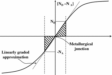
Idealized linearly graded approximation
-
(a)
-
3.
Consider a pn junction with uniform N D on the N-side and N A on the P-side, and narrow widths W n, W p as shown in Fig. 3.14. The ratio of thermal equilibrium electron concentration \(\overline{n}_{\text{p}}\) at the boundary of the depletion layer on the P-side to the electron concentration \(\overline{n}_{\text{n}}\) at the depletion boundary of the N-side and the corresponding relation for holes are given by (3.7).
-
(a)
Assume that when a forward voltage V F is applied to the junction, the barrier is reduced by V F and the relations for electrons follow Boltzmann’s distribution law as
$$n_{\text{p}} = n_{\text{n}} {\text{e}}^{{ - q(V_{\text{bi}} - V_{\text{F}} )/kT}} ;\quad p_{\text{n}} = p_{\text{p}} {\text{e}}^{{ - q(V_{\text{bi}} - V_{\text{F}} )/kT}}$$Use the results to show that
$$\Delta n_{\text{p}} = \overline{n}_{\text{p}} ({\text{e}}^{{qV_{\text{F}} /kT}} - 1);\quad\Delta p_{\text{n}} = \overline{p}_{\text{n}} ({\text{e}}^{{qV_{\text{F}} /kT}} - 1)$$ -
(b)
Assume that the injected excess minority-carrier concentration drops linearly from the depletion edge to the contacts and derive (3.25).
-
(a)
-
4.
A pn junction is made in a 2 Ω-cm resistivity silicon P-type wafer by implanting and diffusing arsenic at the surface such that the N-type region has a concentration of 1020 cm−3. The area of the junction is 100 × 100 μm2. The thickness of the wafer is 750 μm. The trap density in the P-type wafer is N t = 1012 cm−3. Ohmic contacts are made to the N-region and bottom of the wafer. At 25 °C, determine
-
(a)
The thermal equilibrium built-in voltage.
-
(b)
The reverse current for a reverse voltage V R = 5 V.
-
(c)
The forward current for a forward voltage V F = 0.5 V.
-
(d)
The junction capacitance at a reverse voltage V R = 5 V.
-
(e)
The reverse voltage necessary to spread the depletion region 25 mm in the P-region.
-
(f)
The junction breakdown voltage.
-
(a)
-
5.
The concentrations in an abrupt pn junction are N A = N D = 5 × 1018 cm−3. At what reverse voltage will this junction breakdown. Assume that Zener breakdown occurs when the peak field reaches 106 V/cm.
-
6.
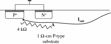
Consider the N+P junction in the figure below. The N+-layer is externally shorted to the P+ substrate contact. Impact ionization in an adjacent circuit generates a hole current that passes under the N+-region and is collected at the substrate contact. The resistance between point A in the substrate immediately under the N+-region and the P+-contact is about 4 kΩ. The average trap density in the substrate is 1012 cm−3, and the wafer temperature is 25 °C.
-
(a)
At what substrate current I sub will the N+P junction develop a forward bias of 0.25 V?
-
(b)
For a forward bias of 0.25 V, what is the excess electron concentration at the depletion boundary in the substrate?
-
(c)
Estimate the diffusion length minority electrons in the substrate.
-
(a)
-
7.
Consider a one-sided N+P step junction having a junction depth of 0.3 μm and a uniform background concentration N A = 1017 cm−3. The effective density of generation-recombination sites in the P-region is 1010 cm−3. An N+-region is placed 0.8 μm below the silicon surface and reverse-biased at 5 V.
-
(a)
Calculate the electron current density for a forward bias voltage of 0.8 V at 25 and 100 °C.
-
(b)
Punch-through occurs when the depletion regions of the top and bottom junction merge in the P-region. The reverse voltage is increased until a current of 1 μA/μm2 is measured. Is the main mechanism for this current impact ionization, punch-through, or thermal generation?
-
(a)
-
8.
A one-sided N+P junction is formed by diffusing a heavily doped N-region to a depth of 0.5 μm into a 10 Ω-cm P-substrate of thickness 725 μm. The density of recombination–generation sites in the P-region is 5 × 1011 cm−3. A forward bias V F = 0.7 V is applied to the junction at 25 °C. Will the minority-carrier electrons reach the backside of the substrate?
-
9.
An abrupt N+P junction is formed by implanting and diffusing arsenic through a 2 × 2 μm2 mask opening into a P-type substrate. The metallurgical junction is 0.25 μm deep, and the substrate is uniformly doped with boron at a concentration of 1017 cm−3. Assume cylindrical junction edges and compare the breakdown voltage at the edge to that in the planar part of the junction at 25 °C.
-
10.
The intrinsic region in a PIN junction is 1 μm thick. Assume that the N-region and P-region are heavily doped. For a reverse voltage, V R = 5 V and 25 °C calculate
-
(a)
The junction capacitance.
-
(b)
The electric field in the intrinsic region.
-
(c)
The transit time for an electron–hole pair generated by a photon at the center of the intrinsic region.
-
(a)


Rights and permissions
Copyright information
© 2015 Springer Science+Business Media New York
About this chapter
Cite this chapter
El-Kareh, B., Hutter, L.N. (2015). PN Junctions. In: Silicon Analog Components. Springer, New York, NY. https://doi.org/10.1007/978-1-4939-2751-7_3
Download citation
DOI: https://doi.org/10.1007/978-1-4939-2751-7_3
Published:
Publisher Name: Springer, New York, NY
Print ISBN: 978-1-4939-2750-0
Online ISBN: 978-1-4939-2751-7
eBook Packages: EngineeringEngineering (R0)