
Abstract
Component mismatch limits the precision of analog circuits, such as converters and current mirrors, and noise ultimately sets a lower limit on signals that can be detected and processed. Both mismatch and noise can have a large impact on the precision of analog and mixed-signal circuits. The first part of this chapter discusses random and systematic mismatch in passive and active components, mismatch characterization, and process and design methods to reduce mismatch. The second part describes the different noise mechanisms, focusing on low-frequency noise and methods to reduce it.
Access this chapter
Tax calculation will be finalised at checkout
Purchases are for personal use only
References
J.-B. Shyu, G. C. Temes, and F. Krummenacher, “Random error effects in matched MOS capacitors and current sources,” IEEE J. Solid-State Circuits, SC-17, 1070-1076, 1982, and SC-19 (6), 948-955, 1984.
K. R. Lakshmikumar, R. A. Hadaway, and M. A. Copeland, “Characterization and modeling of mismatch in MOS transistors for precision analog design,” IEEE J. Solid-State Circuits, SC-21 (6), 1057-1066, 1986.
A. Hastings, The Art of Analog Layout, 254-300, Prentice Hall, 2001.
M. J. M. Pelgrom, A. C. J., Duinmaijer, and A. P. G., Welbers, “Matching properties of MOS transistors,” IEEE J. Solid-State Circuits, 24 (5), 1433-1440, 1989.
P. R. Kinget, “Device mismatch and tradeoffs in the design of analog circuits,” IEEE J. Solid-State Circuits, 40 (6), 1212-1224, 2005.
M. J. M. Pelgrom, H. P. Tuinhout, and M. Vertregt, “Transistor matching in analog CMOS applications,” IEEE IEDM Tech. Digest 915-918, 1998.
M. Steyaert, J. Bastos, R. Roovers, P. Kinget, W. Sansen, B. Graindourze, A. Pergoot, and Er. Janssens, “Threshold voltage mismatch in shortchannel MOS transistors,” Electronics Lett., 30 (18), 1546-1547, 1994.
S. J. Lovett, M. Welten, A. Mathewson, and B. Mason, “Optimizing MOS Transistor Mismatch,” IEEE J. Solid-State Circuits, 33 (1), 147-150, 1998.
G. Baccarani, M. Severi, and G. Soncini, “A new method for the determination of the interface-state density in the presence of statistical fluctuation of the surface potential,” Applied Phys. Lett., 23 (5), 265-267, 1973.
R. Castagne and A. Vapaille, “Apparent interface state density introduced by the spatial fluctuations of surface potential in an M.O.S. structure,” Electronics Lett., 6 (22), 691-693, 1970.
R. W. Keyes, “Physical limits in digital electronics,” Proc. IEEE, 740-768, 1975.
B. Hoeneisen and C. A. Mead, “Fundamental limitations in microelectronics – I. MOS technology,” Solids-State Electron., 15 (7), 819-829, 1972.
K. Takeuchi, T. Tatsumi, and A. Furukawa, “Channel engineering for the reduction of random-dopant-placement-induced threshold voltage fluctuation,” IEEE IEDM Tech. Digest, 841-844, 1997.
P. A. Stolk and D. B. M. Klaassen, “The effect of statistical dopant fluctuations on MOS device performance,” IEEE IEDM Tech. Digest, 627-630, 1996.
T. Mizuno, J.-I. Okamura, and A. Toriumi, “Experimental study of threshold voltage fluctuation due to statistical variation of channel dopant number in MOSFETs,” IEEE Trans. Electron. Dev., 41 (11), 2216-2221, 1994.
A. Asenov and S. Saini, “Polysilicon gate enhancement of the random dopant induced threshold voltage fluctuations in sub-100 nm MOSFETs with ultrathin gate oxide,” IEEE Trans. Electron Dev., 47 (4), 805-812, 2000.
J. A. Croon, H. P. Tuinhout, R. Difrenza, J. Knol, A. J. Moonen, S. Decoutere, H. E. Maes, and W. Sansen, “A comparison of extraction techniques for threshold voltage mismatch,” IEEE ICMTS Tech. Digest, 225-240, 2002.
H. P. Tuinhout, A. H. Montree, and P. A. Stolk, “Effects of gate depletion and boron penetration on matching of deep submicron CMOS transistors,” IEEE IEDM Tech. Digest, 631-634, 1997.
R. Difrenza, J. C. Vildeuil, P. Llinares, and G. Ghibaudo, “Impact of grain number fluctuations in the MOS transistor gate on matching performance,” IEEE ICMTS Tech. Digest, 244-249, 2003.
H. Ryssel, H. Iberl, M. Bleier, G. Prine, K. Haberger, and H. Kranz, “Arsenic-Implanted Polysilicon Layers,” Appl. Phys., 24 (3), 197-200, 1981.
B. Swaminathan, K. C. Saraswat, and R. W.. Dutton, “Diffusion of arsenic in polycrystalline silicon,” Appl. Phys. Lett., 40 (9), 795-798, 1982.
M. Arienzo, Y. Komem, and A. E. Michel, “Diffusion of arsenic in bilayer polycrystalline silicon films,” J. Appl. Phys., 55 (2) 365-369, 1984.
H. Schaber, R. v. Criegern, and I. Weitzel, “Analysis of polycrystalline diffusion source by secondary ion mass spectroscopy,” J. Appl. Phys., 58 (11), 4036-4042, 1985.
J. M. C. Stork, M. Arienzo, and C. Y. Wong, “Correlation between the diffusive and electrical barrier properties of the interface in polysilicon contacted n+-p junctions,” IEEE Trans. Electron Dev., 32 (9), 1766-1770, 1985.
J. L. Hoyt, E. F. Crabbé, R. F. W. Pease, J. F. Gibbons, and A. F. Marshall, “Lateral uniformity of n +/p junctions formed by arsenic diffusion from epitaxially aligned polycrystalline silicon on silicon”, J. Electrochem. Soc., 135 (7), 1773-1779, 1988.
S. Nédèle, D. Mathiot, and M. Gaunneau, “Diffusion of boron on polycrystalline silicon,” ESSDERC Tech. Digest, 153-156, 1996.
A. Wang and K. C. Saraswat, “A strategy for modeling of variations due to grain size in polycrystalline thin-film transistors,” IEEE Trans. Electron Dev., 47 (5), 1035-1043, 2000.
J. T. Horstmann, U. Hilleringmann, and K. F. Goser, “Matching analysis of deposition defined 50-nm MOSFETs,” IEEE Trans. Electron Dev., 45 (1), 299-306, 1998.
T. Tanaka, T. Ususki, T. Futatsugi, Y. Momiyama, and T. Sugii, “Vth fluctuation induced by statistical variation of pocket dopant profile,” IEEE IEDM Tech. Digest, 271-274, 2000.
U. Schaper and J. Enfield, “Matching model for planar bulk transistors with halo implantation,” IEEE Electron Dev. Lett., 32 (7), 589-591, 2011.
J. A. Croon, E. Augendre, S. Decoutere, W. Sanden, and H. E. Maes, “Influence of doping profile and halo implantation on the threshold voltage mismatch of a 0.13 μm CMOS technology,” ESSDERC, 579-582, 2002.
K. Rochereau, R. Difrenza, J. McGinley, O. Noblanc, C. Julien, S. Parihar, and P. Llinares, “Impact of pocket implant on MOSFET mismatch for advanced CMOS technology,” IEEE ICMTS, 123-126, 2004.
C. M. Mezzomo, A. Bajolet, A. Cathignol, and G. Ghibaudo, “Drain current variability in 45 nm heavily pocket-implanted bulk MOSFET,” ESSDERC, 122-125, 2010.
S. Winkelmeier, M. Sarstedt, M. Ereken, M. Goethals, and K. Ronse, “Metrology method for the correlation of line edge roughness for different resists before and after etch,” Microelectronics Eng., 57-58, 665-672, 2001.
S. Xiong and J. Bokor, “A simulation study of gate line edge roughness effects on doping profiles of short-channel MOSFET devices,” IEEE Trans. Electron Dev., 51 (2), 228-232, 2004.
L. H. A. Leunissen, M. Ercken, G. P. Patsis, “Determining the impact of statistical fluctuations on resist line edge roughness,” Microelectronic Eng., 78–79, 2–10, 2005.
C. H. Diaz, H.-J. Tao, Y.-C. Ku, A. Yen, and K. Young, “An experimentally validated analytical model for gate line-edge roughness (LER) effects on technology scaling,” IEEE Electron Dev. Lett., 22 (6), 287-289, 2001.
T. Linton, M. Chandhok, B. J. Rice, and C. Schrom, “Determination of the line edge roughness specification for 34 nm devices,” IEEE IEDM Tech. Digest, 303-306, 2002.
J. A. Croon, G. Storms, S. Winkelmeier, I. Pollentier, M. Ercken, S. Decoutere, W, Sansen, and H. E. Maes, “Line edge roughness: Characterization, modeling and impact on device behavior,” IEEE IEDM Tech. Digest, 307-310, 2002.
G. Declerck, “A look into the future of nanoelectronics,” Symp. VLSI Tech. Digest, 6-10, 2005.
M. Steyart, J. Bastos, R. Roovers, P. Kinget, W. Samsen, B. Graindourze, A. Pergoot, and Er. Janssens, “Threshold voltage mismatch in short-channel MOS transistors,” Electronic Lett., 30 (18), 146-148, 1994.
R. W. Keyes, “High-mobility FET in strained silicon,” IEEE Trans. Electron Dev., ED-33 (6), 853, 1986.
K. Rim, J. L. Hoyt, and J. F. Gibbons, “Fabrication and analysis of deep submicron strained-Si N-MOSFETs,” IEEE Trans. Electron Dev., 47 (7), 1406-1415, 2000.
S. E. Thompson, M. Armstrong, C. Auth, M. Alavi, M. Buchler, R. Chau, S. Cea, T. Ghani, T. Hoffman, C.-H. Jan, C. Kenyon, J. Klaus, K. Kuhn, Z. Ma, B. Mcintyire, K. Mistry, A. Murthy, B. Obradovic, R. Nagisetty, P. Nguyen, S. Sivakumar, R. Shaheed, L.. Shifren, B. Tufts, S. Tyagi, M. Bohr, and Y. El-Masry, “A 90-nm logic technology featuring strained-silicon,” IEEE Trans. Electron Dev., 51 (11), 1790-1796, 2004.
G. Scott, J. Lutze, M. Rubin, F. Nouri, and M. Manley, “NMOS drive current reduction by transistor layout and trench induced stress,” IEEE IEDM Tech. Digest, 827-830, 1999.
P. G. Drennan, M. L. Kniffin, and D. R. Locascio, “Implications of proximity effects for analog designs,” Custom Integrated Circuits Conference (CICC), 169-176, 2006.
K.W. Su, Y.M. Sheu, C.K. Lin, S.J. Yang, W.J. Liang, X. Xi, C.S. Chiang, J. K. Her, Y. T. Chia, C. H. Diaz, and C. Hu, “A scaleable model for STI mechanical stress effect on layout dependence of MOS electrical characteristics,” Custom Integrated Circuits Conference (CICC), 245-248, 2003.
R. A. Bianchi, G. Bouche, O. Roux-dit-Buisson, “Accurate modeling of trench isolation induced mechanical stress effects on MOSFET electrical parameters,” IEEE IEDM Tech. Digest, 117-120, 2002.
N. Wils, H. P. Tuinhout, and M. Meijer, “Characterization of STI edge effects on CMOS variability,” IEEE Trans. Semiconductor Manufacturing, 22 (1), 59-65, 2009.
T. B. Hook, J. Brown, P. Cottrell, E. Adler, D. Hoyniak, J. Johnson, and R. Mann, “Lateral ion implant straggle and mask proximity effect”, IEEE Trans Electron Dev., 50 (9), 1946-1951, 2003.
T. Kanamoto, Y. Ogasahara, K. Natsume∗, K. Yamaguchi, H. Amishiro, T. Watanabe, and M. Hashimoto, “Impact of well edge proximity effect on timing,” Device Research Conf., 115-118, 2007.
Y. M. Sheu, K. W. Su, S. J. Yang, H. T. Chen, C. C. Wang, M. J. Chen, and S. Liu, “Modeling well edge proximity effect on highly-scaled MOSFETs,” IEEE Custom Integrated Circuits Conf. , 831-834, 2005.
J. Watts, K. W. Su, and M. Basel, “Netlisting and modeling well-proximity effects,” IEEE Trans. Electron Dev., 53 (9), 2179-2196, 2006.
A. R. Brown, G. Roy, and A. Asenov, “Poly-Si-gate-related variability in decananometer MOSFETs with conventional architecture,” IEEE Trans. Electron Dev., 54 (11) 3036-3063, 2007.
H. Tuinhout, M. Pelgrom, R. Penning de Vries, and M. Vertregt, “Effects of metal coverage on MOSFET matching,” IEEE IEDM Tech. Digest, 735-738, 1997.
X. Wu, J. Trogolo, F. Inoue, Z. Chen, P. Jones-Williams, I. Khan, and P. Madhani, “Impact of sinter process and metal coverage on transistor mismatching and parameter variations in analog CMOS technology” IEEE ICMTS Tech Digest, 69-73, 2007.
P. G. Drennan, C. C. McAndrew, and J. Bates, “A comprehensive vertical BJT mismatch model,” IEEE BCTM Tech. Digest., 83-86, 1998.
H. P. Tuinhout, “Improving BiCMOS technologies using BJT parametric mismatch characterization, ”IEEE BCTM Tech. Digest, 163-170, 2003.
P. G. Drennan, C. C. McAndrew,, J. Bates, and D. Schroder, “Rapid evaluation of the root causes of BJT mismatch,” IEEE BCTM Tech. Digest, 122-127, 2000.
C. McAndrew, J. Bates, T. T. Ida, and P. Drennan, “Efficient statistical BJT modeling, why β is more than IC/IB,” IEEE BCTM Tech. Digest, 28-31, 1997.
S. Bordez, S. Danaie, R. Difrenza, J.-C. Vildeuil, and G. Morin, “Study of bipolar matching at high current level with various test configurations leading to a new model approach,” IEEE BCTM Tech. Digest, 62-65, 2005.
P. G. Drennan, “Diffused resistor mismatch modeling and characterization,” IEEE BCTM Tech. Digest, 27-30, 1999.
F. Larsen, M. Ismail, and C. Abel, “A versatile structure for on-chip extraction of resistance matching properties,” IEEE Trans. Semiconductor Manufacturing, 9 (2), 281-285, 1996.
R. Thewes, R. Brederlow, C. Dahl, U. Kollmer, C. G. Linnenbank, B. Holzapfl, J. Becker, J. Kissing, S. Kessel, and W. Weber, “Explanation and quantitative model for the matching behavior of poly-silicon resistors,” IEEE IEDM Tech Digest., 771-774, 1998.
H. Thibieroz, P. Shaner, and Z. C. Butler, “Mismatch and flicker noise characterization of tantalum nitride thin film resistors for wireless applications,” IEEE ICMTS Tech Digest, 207-212, 2001.
U. Grünebaum, J. Oehm, and K. Schumacher, “Mismatch modeling and simulation – a comprehensive approach,” Analog Integrated Circuits and Signal Processing, Kluwer Academic Publishers, 29, 165-171, 2001.
H. Iwai and S. Kohyama, “On-chip capacitance measurement circuits in VLSI structures,” IEEE Trans. Electron Dev., ED-29 (10), 1622-1626, 1982.
B. Eitan, “Channel-length measurement technique based on a floating-gate device,” IEEE Electron Dev. Lett., 9 (7), 340-342, 1988.
C. Kortekaas, “On-chip quasi-static floating-gate capacitance measurement method,” IEEE ICMTS Tech. Digest, 109-113, 1990.
H. P. Tuinhout, H. Elzinga, J. T. Brugman, and F. Postma, “Accurate capacitor matching measurements using floating gate test structures,” IEEE ICMTS Tech. Digest, 133-137, 1995.
H. P. Tuinhout, H. Elzinga, J. T. Brugman, and F. Postma, “The floating gate measurement technique for characterization of capacitor matching,” IEEE Trans. Semicon. Manuf. 9 (1), 2-8, 1996.
J. Hunter, P. Gudem, and S. Winters, “A differential floating gate capacitance mismatch measurement technique,” IEEE ICMTS Tech. Digest 142-147, 2000.
W. Tian, J. Trogolo, R. Todd, and L. Hutter, “Gate oxide leakage and floating gate capacitor matching test,” IEEE ICMTS Tech. Digest, 19-22, 2007.
A. van der Ziel, Noise in Solid State Devices and Circuits, John Wiley & Sons, 1986.
M. von Haartman and M. Östling, Low-Frequency Noise in Advanced NOS Devices, Springer, 2007.
A. L. McWhorter, “1/f noise and germanium surface properties,” in Semiconductor Surface Physics, R. H. Kingston, Editor, University of Pennsylvania Press, 207-228, 1957.
F. N. Hooge, “1/f noise,” Physica, 83B, 14-23, 1976.
H. Nyquist. Thermal Agitation of Electric Charge in Conductors. Phys. Rev., 32 (1), 110-113, 1928.
J. B. Johnson. Thermal Agitation of Electricity in Conductors. Phys. Rev., 32 (1), 97-109, 1928.
W. Schottky, “Ueber spontane Stromschwankungen in vershiedenen Elektrizitaetsleitern,” (On the spontaneous current fluctuations in different conductors,” Annalen der Physik, 57, 541-567, (1918).
M. J. Kirton and M. J. Uren, “Noise in solid-state microstructures: A new perspective on individual defects, interface states and low-frequency (1/f) noise,” Advances in Physics, 38 (4), 367-468, 1989.
K. Kandiah and F. B. Whiting, “Low frequency noise in junction field-effect transistors,” Solid-State Electronics, 31 (8), 1079-1088, 1978.
R. C. Jaeger and A. J. Brodersen, “Low frequency noise sources, in bipolar junction transistors,” IEEE Trans. Electron Dev., ED-17 (2), 128-134, 1970.
M. J. Kirton, M. J. Uren, and S. Collins, “Individual interface states and their implication for low-frequency noise in MOSFETs,” Appl. Surf. Science, 30 (1-4), 148-152, 1987.
C. Surya and T. Y.Hsiang, “Surface mobility fluctuations in metal-oxide-semiconductor field-effect transistors,” Phys. Rev. B., 35 (12), 6343-6347, 1987.
K. K. Hung, P. K. Ko, C. Hu, and Y. C. Cheng, “Random telegraph noise of deep-submicrometer MOSFETs,” IEEE Electron Dev. Lett., 11 (2), 90-92, 1990.
K. S. Ralls, W. J. Skocpol, L. D. Jackel, R. E. Howard, L. A. Fetter, R. W. Epworth, and D. M. Tennant, “Discrete resistance switching in submicrometer silicon inversion layers: individual interface traps and low-frequency (1/f?) noise,” Phys. Rev. Lett., 52 (3), 228-231, 1984.
M. J. Uren, D. J. Day, and M. J. Kirton, “1/f and random telegraph noise in silicon metal-oxide-semiconductor field-effect transistors,” Appl. Phys. Lett., 47 (11), 1195-1197, 1985.
Y. F. Lim, Y. Z. Xiong, N. Singh, R. Yang, Y. Jiang, D. S. H. Chan, W. Y. Loh, L. K. Bera, G. Q. Lo, N. Balasubramanian, and D. -L. Kwong, “Random telegraph signal noise in gate-all-around Si-FinFET with ultra-narrow body,” IEEE Trans. Electron Dev., 77 (9), 765-768, 2006.
S.-R. Li, W. McMahon, Y.-L. R. Lu, and Y.-H. Lee, “RTS noise characterization in flash cells,“ IEEE Electron Dev. Lett., 29 (1), 106-108, 2008.
C. M. Compagnoni, R. Gusmeroli, A. S. Spinelli, and A. Visconti, “RTN VT instability from the stationary trap-filling condition : An analytical spectroscopic investigation,” IEEE Trans. Electron Dev., 55 (2), 655-661, 2008.
R. H. Howard, W. J. Skocpol, L. D. Jackel, P. M. Mankiewich, L. A. Fetter, D. M. Tennant, R. Epworth, and K. S. Ralls, “Single electron switching events in nanometer-scale Si MOSFETs,” IEEE Trans. Electron Dev., ED-32 (9), 1669-1674, 1985.
S. Machlup, “Noise in semiconductors: spectrum of a two-parameter random signal,” J. Appl. Phys., 25, 241-243, 1954.
J. L. Plumb and E. R. Chenette, “Flicker noise in transistors,” IEEE Trans. Electron Dev., 10 (5), 304-308, 1963.
O. Roux dit Buisson and G. Moria, “Flicker noise characteristics of polysilicon resistors in submicron BiCMOS technologies,” IEEE ICMTS Tech. Digest, 49-51, 1997.
E. Zhao, R. Krithivasan, A. K. Sutton, Z. Jin, J. D. Cressler, B. El-Kareh, S. Balster, and H. Yasuda, “An investigation of low-frequency noise in complementary SiGe HBTs,” IEEE Trans. Electron Dev., 53 (2), 329-338, 2006.
F. N. Hooge, T. G. M. Kleinpenning, and L. K. J. Vandamme, “Experimental studies on 1/f noise,” Rep. Prog. Phys., 44, 479-531, 1981.
P. Dutta and P. M. Horn, “Low-frequency fluctuations in solids: 1/f noise,” Rev. Mod. Phys., 53, 497-516, 1981.
Klaassen, F.M., “Characterization of low 1/f noise in MOS transistors’, IEEE Trans. Electron Dev., ED-18 (10), pp. 887–891, 1971.
G. Ghibaudo, O, Roux, C.N. Duc, F. Balestra, and J. Brini, “Improved analysis of low frequency noise in field-effect MOS transistors’, Phys. Status Solidi (a), 124-128,. 571–581, 1991.
K. K. Hung, P. K. Ko, C. C. Hu, and Y. C. Cheng, “A unified model for the flicker noise in metal-oxide-semiconductor field-effect transistors”, IEEE Trans. Electron Dev., 37, (3), 654–665, 1990.
S. Christensson, I. Lundstrom, and C. Svensson, “Low frequency noise in m.o.s. transistor. Pt. I—Theory, Pt. II—Experiments”, Solid-State Electronics, 11, 797-820, 1968.
C. T. Sah and F. H. Hielscher,:”Evidence of the surface origin of the 1//noise”, Phys. Rev. Lett., 17, 956-, 1966.
K. S. Ralls, W. J. Skocpol, L. D. Jackel, R. E. Howard, L. A. Fetter, R. W. Epworth, and D. M. Tennant, “Discrete resistance switching in submicrometer silicon inversion layers: individual interface traps and low-frequency (1/f?) noise,” Phys. Rev. Lett., 52 (3), 228-231, 1984.
T. Boutchacha, G. Ghibaudo, and B. Belmekki, “Study of low frequency noise in the 0.18 μm silicon CMOS transistors,” IEEE ICMTS Tech. Digest, 84–88, 2004.
M. Valenza, A. Hoffmann, D. Sodini, A. Laigle, F. Martinez and D. Rigaud, “Overview of the impact of downscaling technology on 1/f noise in p-MOSFETs to 90 nm,” IEEE Proc. Circuits, Devices, and Systems, 151 (2), 102-110, 2004.
J. Chang, A. A. Abidi, and C. R. Viswanathan, “Flicker noise in CMOS transistors from subthreshold to strong inversion,” IEEE Trans. Electron Dev., 41 (11), 1965-1971, 1994.
B. El-Kareh and J. H. Kim, “Low-frequency noise in precision analog components,” Korean Conference on Semiconductors (KCS), Seoul, Korea, May 2012.
R. Brederlow, W. Weber, R. Jurk, C. Dahl, S. Kessle, J. Holz, W. Sauer, P. Klein, B. Lemaire, D. Schmitt-Landsieldel, and R. Thewes, “Influence of fluorinated gate oxides on the low frequency noise of MOS transistors under analog operation,” ESSDERC, 472-475, 1998.
M. M. Nelson, K. Yokoyama, M. Thomason, G. Scott, and B. Greenwood, “Efficacy of fluorine doping at various stages on noise reduction,” IEEE Worshop on Microelectr. and Electron Dev. (WMED), 17-20, 2005.
T. P. Ma, “Metal-oxide-semiconductor gate oxide reliability and the role of fluorine,” J. Vac. Sci. Tech., A-10, 705-712, 1992.
A. Balasinski, M. H. Tsai, L. Vishnuhotta, T. P. Ma, H. H. Tseng, and P. J. Tobin, “Interface properties in fluorinated (100) and (111) Si/SiO2 MOSFETs,” Microelectr. Eng., 22, 97-100, 1993.
P. Wright and K. C. Saraswat, “The effect of fluorine in silicon dioxide gate dielectrics,” IEEE Trans. Electron Dev., 36 (5), 879-889, 1989.
J. R. Pfiester, F. K. Baker, T. C. Mele, H. H. Tseng, P. J. Tobin, J. D. Hyden, J. W. Miller, C. D. Gunderson, and L. C. Parrillo, “The effects of boron penetration on p+ polysilicon gated PMOS devices,” IEEE Trans. Electron Dev., 37 (8), 1842-1850, 1990.
J. J. Sung and C. Y. Lu, “A comprehensive study on p + polysilicon-gate MOSFET’s instability with fluorine incorporation,” IEEE Trans. Electron Dev., 37 (11), 2312-2320, 1990.
M. Cao, P. V. Voorde, M. Cox, and W. Greene, “Boron diffusion and penetration in ultrathin oxide with poly-Si gate,” IEEE Electron Dev. Lett., 19 (8), 291-293, 1998.
K. A. Ellis and R. A. Buhrman, “Nitrous oxide (N2O) processing for silicon oxynitride gate dielectrics,” IBM J. Res. Dev. 43 (3), 287-300, 1999.
M. Marin, J. C. Vildeuil, B. Tavel, B. Duriez, F. Arnaud, P. Stolk, and M. Woo,” Can 1/f noise in MOSFETs be reduced by gate oxide and channel optimization?,” Proc. Intnl. Conf. Noise and Fluctuations -ICNF, 195-198, 2005.
K.W. Chew, K.S. Yeo, and S.-F. Chu, “Impact of technology scaling on the 1/f noise of thin and thick gate oxide deep submicron NMOS transistors,” IEE Proc.-Circuits Devices Syst., 151 (5), 415-421, 2004.
P. Morfouli, G. Ghibaudo, T. Ouisse, E. Vogel, W. Hill, V. Misra, P. McLarty, and J. J. Wortman, “Low-frequency noise characterization of n- and p-MOSFET’s with ultrathin oxynitride gate films,” IEEE Trans. Electron Dev., 17 (8), 395-397, 1996.
R. Jayaraman and G. C. Sodini, “1/f noise interpretation of the effect of gate oxide nitridation and reoxidation in dielectric traps”, IEEE Trans. Electron Devices, 37, (1), 305–309, 1990.
G. Lucovsky, “Ultrathin nitrided gate dielectrics: Plasma processing, chemical characterization, performance, and reliability,” IBM J. Res. Dev., 43 (3), 301-326, 1999.
M. Da Rold, E. Smoen, S. Mertens, M. Schaekers, G, Badenes, and S. Decoutere, “Impact of gate oxide nitridation process on 1/f noise in 0.18 mm CMOS,” Microelectron. Reliab., 41, 1933-1938, 2001.
R. V. Wang, Y. H. Lee, Y. L. R. Lu, W. McMahon, S. Hu, A. Ghetti, “Shallow Trench Isolation Edge Effect on Random Telegraph Signal Noise and Implications for Flash Memory,” IEEE Trans. Electron Dev., 56 (9), 2107-2113 , 2009.
C. Y. Chan, Y. S. Lin, Y. C. Huang, S. S. H. Hsu, and Y. Z. Juang, “Impact of STI effect on flicker noise in 0.13 mm nMOSFETs,” IEEE Trans Elecron Dev., 54 (12) m 3383-3392, 2007.
P. Srinivasan, W. Xiong, and S. Zhao, “Low-frequency noise in integrated N-well resistors,” IEEE Electron DEv.Lett., 31 (12) , 1476-1478, 2010.
F. N. Hooge, T. G. M. Kleinpenning, and L. K. J.Vandamme, “Experimental studies on l/f noise,” Reports on Progress in Physics, 44,(5), 479-532, 1981.
F. N. Hooge,”1/f noise is no surface effect”, Phys. Lett. A 29, 141-141, 1969.
L. K. Vandamme and H. H. Casier, “The 1/f noise versus sheet resistance in poly-Si is similar to poly-SiGe resistors and Au-layers,” ESSDERC, 365-368, 2004.
K. M. Chen, G.W. Huang, J. F. Kuan, H.. J. Huang, C. Y. Chang, and T. H. Yang, “Low Frequency Noise in Boron Doped Poly-SiGe Resistors,” MTT-S, 405-408, 2002.
R. Brederlow, W. Weber, C. Dahl, D. Schmitt-Landsiedel, and R. Thewes,”Low-Frequency Noise of Integrated Poly-SiliconResistors,” IEEE Trans. Electron Dev., 48 (6), 1180-1187, 2001.
M. Da Rold, S. Van Huylenbroek, B. Knuts, E. Simoen, and S. Decoutere, “On the basic correlation between polysilicon resistor linearity, matching and 1/f noise,” ESSDERC, 448-651, 1999.
H. Thibieroz, P. Shaner, and Z. C.elik Butler, “Mismatch and flicker Noise characterization of tantalum nitride thin film resistors for wireless applications,” IEEE ICMTS Tech. Digest, 287-212, 2001.
G. Niu, “Noise in SiGe HBT RF technology: Physics, modeling, and circuit implications,” Proc. IEEE, 93 (9), 1583-1597, 2005.
“Integration of a Complementary-SiGe BiCMOS Process for High-Speed Analog Application”, Silicon Heterostructure Handbook, John Cressler, Editor, CRC Press, July 2005.
B. El-Kareh, S. Balster, W. Leitz, P. Steinmann, H. Yasuda, M. Corsi, K. Dawoodi, C Dirnecker, P. Foglietti, A. Haeusler, P. Menz, M. Ramin, T. Scharnagl, M. Schiekofer, M. Schober, U. Schulz, L. Swanson, D. Tatman, M. Waitschull, J. W. Weijtmans, and C. Willis, “.A 5 V complementary-SiGe BiCMOS technology for high-speed precision analog circuits,” IEEE Proc. BCTM, 211-214, 2003.
W. E. Zhao, A. K. Sutton, B. M. Haugerud, J. D. Cressler, P. W. Marshall, R. A. Reed, S. G. Balster, H. Yasuda, and B. El-Kareh “The Effect of Radiation on 1/f Noise in Complementary (NPN + PNP) HBTs”, IEEE Trans. Nuclear Science, 51 (6), 3243-3249, 2004.
P. T. Gray, P. J. Hurst, S. H. Lewis, and R. G. Meyer, Analysis and Design of Analog Integrated Circuits, John Wiley & Sons, 330-332, 2001.
R. J. Baker, CMOS Circuit Design, Layout, and Simulations, John Wiley & Sons, IEEE press, 613-616, 2010.
B. Wang, J. M. Hellums, and C. G. Sodini, “MOSFET thermal noise modeling for analog integrated circuits,” IEEE JSSC, 29 (7), 833-835, 1994.
Author information
Authors and Affiliations
Corresponding author
Problems
Problems
The temperature is 300 K unless otherwise stated.
-
1.
An NMOS pair exhibits a standard deviation of threshold voltage mismatch, \(\sigma_{{\Delta V_{\text{T}} }} ,\) of 10 mV. Scattering of phosphorus during implantation causes the effective doping concentration in the channel of one NMOS to increase by 1010 cm−2 while the other NMOS remains unaffected. Assume a long and wide channel and an equivalent oxide thickness of 12.5 nm and sketch the distribution of a large number of mismatch measurements.
-
2.
The figure below shows two N-well resistors that are identically constructed in a P-substrate, except for a degenerately doped poly conductor crossing one of the resistors. Assume a uniform N-well phosphorus concentration of 5 × 1016 cm−3, a uniform P-substrate boron concentration of 5 × 1014 cm−3, and disregard edge effects. Estimate the systematic mismatch between the two resistors (Fig. P2).
Fig. P2 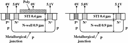
N-well resistor matching problem 5.2
-
3.
Two identical MOSFETs are connected with first metal and operated in the linear mode. The metal line connecting the common source to ground is 50-μm long and 10-μm wide, and the metal lines connecting the MOSFET drains are 50-μm long and 20-μm wide on one MOSFET and 50-μm long and 0.25-μm wide on the other. Describe qualitatively how this design would affect mismatch.
-
4.
Consider the array of polysilicon resistors of a uniform sheet resistance 250 Ω/□ in Fig. P4. The resistor-body length body is L = 10 μm and its drawn width and space, respectively, W = 0.5 μm and S = 0.5 μm. The measured resistance is 6250 Ω at each end of the array and 5000 Ω at the array center. Assume the difference to be solely due to a linear gradient in over-etch, and
-
(a)
Find the etch-bias per resistor edge.
-
(b)
Plot the systematic mismatch as a function of distance between array center and array edge.
Fig. P4 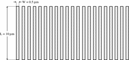
Polysilicon resistor matching problem 5.4
-
(a)
-
5.
Calculate the shot noise in a diode current of 1.5 mA in a bandwidth of 1 MHz.
-
6.
The power spectral density of the noise voltage is measured as 2.5 × 10⁻¹⁶ V2/Hz for a bandwidth of 1 MHz. Find the root-mean-square of the noise voltage.
-
7.
A polysilicon resistor has a resistance of 250 Ω, what is the PSD of the thermal noise voltage 300 K?
-
8.
The resistor in Problem 5.6 shows a flicker noise PSD of 3.2 × 10⁻¹⁹ A2/Hz. Find the root-mean-square of current noise in the bandwidth 10 Hz–1 kHz.
-
9.
The flicker noise is measured on an NMOSFET as \(S_{{I_{\text{D}} }}\) = 5 × 10⁻¹⁷ A2/Hz at 100 Hz, V G − V T = 2.5 V, and I D = 5 mA. The channel length and width are, respectively, 0.6 and 10 μm. For an equivalent oxide thickness t eq = 12.5 nm, estimate the effective oxide trap density and the input-referred voltage noise.


Rights and permissions
Copyright information
© 2015 Springer Science+Business Media New York
About this chapter
Cite this chapter
El-Kareh, B., Hutter, L.N. (2015). Mismatch and Noise. In: Silicon Analog Components. Springer, New York, NY. https://doi.org/10.1007/978-1-4939-2751-7_10
Download citation
DOI: https://doi.org/10.1007/978-1-4939-2751-7_10
Published:
Publisher Name: Springer, New York, NY
Print ISBN: 978-1-4939-2750-0
Online ISBN: 978-1-4939-2751-7
eBook Packages: EngineeringEngineering (R0)