
Abstract
Real photovoltaic converters (solar cells ), consisting of molecular, liquid, or solid state structures of various types, exhibit particular departures from the ideal converter presented in Chap. 4 These departures concern for example:
-
Incomplete absorption of solar photons with energies above the optical threshold energy.
-
Considerable rates of non-radiative transitions from excited states to the ground states, commonly introduced by defects, dopants, impurities, surface states, and interface states.
-
Limitations of transport of charge carriers or excitonic compounds that move the photoexcited states to the boundaries of the absorber and connect them to leads to the outside.
Access this chapter
Tax calculation will be finalised at checkout
Purchases are for personal use only
Notes
- 1.
For infinite p- and n-type doped layers, it is assumed that the finite number of electrons and holes having moved across the junction are distributed within the infinite layer lengths without increasing the overall initial thermal-equilibrium majority carrier concentrations.
- 2.
Each of the core levels of the atoms in the p- and n-type doped regimes are spatially modulated by this potential function \(\varphi (x)\).
- 3.
If the thickness of the semiconductor is less than the width of the space-charge region, the surplus of charges needed for chemical equilibrium is located in the outer metal contacts of the device.
- 4.
Regardless of its mode of operation (except for particularly extreme cases which are irrelevant for our purposes), the space-charge region of a diode exhibits spatial gradients in the conduction and valence bands. These gradients also exist in thermal equilibrium (no illumination, no applied voltage, etc.), where—in accordance with the second law of thermodynamics—definitely no current can flow. Here we do not discuss Brownian motion, which does not contribute to stationary carrier flows.
- 5.
We may also regard the extension of the electron and hole-wave functions which are extended infinitely in the infinite device for energies ε ≥ ε C,p-side for electrons and ε ≤ ε V,n-side for holes.
- 6.
Diffusion of a particular species originates from the spatial gradient of their concentration \(n(\mathbf{x})\). The resulting flux Γ reads \(\boldsymbol{\varGamma }(\mathbf{x}) = D\big[-\nabla n(\mathbf{x})\big]\), where D is the diffusion coefficient . The spatial density \(n(\mathbf{x})\) is derived by solving the steady-state continuity equation
$$\displaystyle{\nabla {\boldsymbol \cdot }\big[n(\mathbf{x})\mathbf{u}(\mathbf{x})\big] = \nabla \boldsymbol{\cdot \varGamma } (\mathbf{x}) = g(\mathbf{x}) - r(\mathbf{x})\;.}$$With carrier velocity \(\mathbf{u}(\mathbf{x})\) generation rate \(g(\mathbf{x}) = 0\) and recombination rate given by the quotient of the density \(n(\mathbf{x})\) and the lifetime τ, viz., \(r(\mathbf{x}) = n(\mathbf{x})/\tau\), we arrive at the second order differential equation
$$\displaystyle{\nabla {\boldsymbol \cdot }\big[-D\nabla n(\mathbf{x})\big] = -D\Delta n(\mathbf{x}) = -\frac{n(\mathbf{x})} {\tau } \;.}$$In one dimension, this has the general solution
$$\displaystyle{n(x) = A\exp \left (+ \frac{x} {\sqrt{D\tau }}\right ) + B\exp \left (- \frac{x} {\sqrt{D\tau }}\right )\;.}$$The length \(\sqrt{D\tau } = L\) is called the diffusion length . In the case considered here, for infinite extension of the p-type regime (towards x → −∞) and n-type region (towards x → +∞), only one of the terms of the solution meets the boundary condition of density n approaching zero at infinite distances from the junction, and we arrive at n(x) decaying purely exponentially either in x < 0, or in x > 0.
- 7.
See, for example, the recombination in a 3-level system, as discussed in detail in [6].
- 8.
We immediately recognize with ξ < 1 for the arguments in the ln-functions \(\left [\xi \varDelta n(n_{0} + p_{0}) +\xi ^{2}(\varDelta n)^{2}\right ] < \left [\varDelta n(n_{0} + p_{0}) + (\varDelta n)^{2}\right ]\), and remember the natural logarithm to be a monotonous function to find the ratio of the respective ln-functions.
- 9.
When looking at the peak of the np-product more closely, we have neglected the contribution of the comparatively weak dependence of the densities of states on energy (\(D(\epsilon ) \sim \sqrt{\epsilon }\).
- 10.
In this approach (named SHR-approach after Shockley, Read, and Hall) the recombination rate depends on the carrier concentrations in the bands U ∽ np and accordingly the transition is radiative.
- 11.
Diode factors n > 1 by all appearances are usually interpreted to reflect losses of additional irreversible effects in recombination and transport.
- 12.
In this analytical approach for the determination of the ∇ε Fn, we only require information about the local behavior of ε C(ξ) and ε Fn(ξ). Of course, we gain no knowledge of the ‘outer’ magnitudes of the device, such as current density, applied voltage, etc.
- 13.
Of course, the local excess concentration \(\Delta n(\xi ) = g_{0}^{{\ast}}\tau ^{{\ast}}\) results from photogeneration, and respective motion and recombination of electrons; however, we neither need to know, nor we are interested in the details of its development.
- 14.
As the voltage in the short circuit mode (V bi) and under bias, e.g. forward bias (V ext > 0) drops across the space charge region, we may qualitatively compare V bi and V ext instead of \(\bigtriangledown \epsilon _{\mathrm{C}}\) and \(\bigtriangledown \epsilon _{\mathrm{Fn}}\).
- 15.
The thermal equilibrium concentration n is the ‘enemy’ of the excited state characterized by an excess density \(\Delta n\) when entering into the chemical potential
$$\displaystyle{\mu = \mathit{kT}\ln \left [\frac{\Delta n + n} {n} \right ]\;.}$$ - 16.
For the correct reproduction of a heterojunction band diagram, and in particular for the band behavior at the interface, the different dielectric functions of the individual layers have to be considered.
- 17.
Semiconductors with significantly disturbed translational symmetry, such as amorphous or microcrystalline silicon thin films (a-Si:H, μc-Si:H) and their corresponding alloys with other group IV elements like Si-Ge- and Si-C-alloys show such low mobility and low diffusion lengths.
- 18.
We have to keep in mind that the quantity ‘electric field’ \(E_{x} = -\int \rho (x)\mathrm{d}x\) does not represent the correct driving force for charge carriers.
- 19.
For the complete device on needs, of course, a transparent front contact.
- 20.
The tunneling probability through barriers that are linearly dependent on spatial coordinates is represented by solutions of the two branches of the Airy-type differential equation.
- 21.
In order to avoid immediate recombination of excited electrons and holes in the absorber molecule, electrons and holes are transferred with energetic relaxation, Δ L (for electrons from the LUMO level) and Δ H (for holes from the HOMO level) to their respective transport levels (ε el,cond, ε hole,cond).
- 22.
Geminate recombination refers to the ‘immediate’ back reaction of species, e.g., weakly bound photogenerated electrons and holes (excitons) in terms of a radiative transition to the ground state.
- 23.
Although the absorption coefficient of molecular dyes generally may exceed those of semiconductors the effective thickness of dye layers—due to low exciton diffusion lengths—is usually chosen much lower so that full absorption A → 1 might not be achieved.
- 24.
Overpotential (Δ i) designates the departure of the potentials of an electrode system from its chemical equilibrium value. Such a departure is required to create a net chemical reaction; the larger (Δ i) the larger the reaction rate.
- 25.
The ‘resistors’ r p and r s are expressed in terms Ohm cm2, as in the sketches in Fig. 5.40.
Fig. 5.40 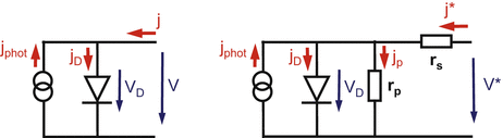
Equivalent circuits of an illuminated ideal diode (left) and a diode with parallel and series resistors representing losses by non-radiative recombination (r p) and non-ideal leads (r s) (right)

References
S.M. Sze, Physics of Semiconductor Devices (Wiley, New York, 1981)
B. Sapoval, C. Hermann, Physics of Semiconductors (Springer, Berlin, 2003)
R. Enderlin, N.J.M. Horing, Fundamentals of Semiconductor Physics and Devices (World Scientific, Singapore, 1997)
R. Sauer, Halbleiterphysik (Oldenbourg, München, 2009)
H.G. Wagemann, H. Eschrich, Grundlagen der photovoltaischen Energiewandlung (Teubner, Stuttgart, 2010)
W. Shockley, W.T. Read, Phys. Rev. 87, 835 (1952); R.N. Hall, Phys. Rev. 87, 387 (1952)
J.S. Yuan, J.J. Liou, Semiconductor Device Physics and Simulation (Plenum, New York, 1998)
P. Würfel, The Physics of Solar Cells (Wiley-VCH, Weinheim, 2009)
D.V. Morgan, R.H. Williams, Physics and Technology of Heterojunction Devices (P. Peregrinus Ltd, London, 1991)
W. Schottky, Zeitschr. Physik 118, 539 (1942)
H.K. Henisch, Semiconductor Contacts (Clarendon Press, Oxford, 1984)
C.W. Tang, Appl. Phys. Lett. 48, 183 (1986)
G. Yu et al., Science 270, 1789 (1995)
M. Granström et al., Nature 395, 257 (1998)
K. Yoshino et al., IEEE Trans. Electron Dev. 44, 1315 (1997)
P. Fulde, Electron Correlations in Molecules and Solids (Springer, Berlin, 1995)
U. Bach et al., Nature 395, 583 (1998)
M. Graetzel, MRS-Bull. 30, 23 (2005)
J. Kroon, A. Hinsch, Dye-sensitized solar cells, in Organic Photovoltaics, ed. by C. Brabec et al. (Springer, Berlin, 2003)
B.A. Gregg, J. Appl. Phys. 93, 3605 (2003)
S.R. Forest, MRS-Bull. 30, 28 (2005)
C. Hamaguchi, Basic Semiconductor Physics (Springer, Berlin, 2001)
M.A. Green, K. Emery, Y. Hishikawa, W. Warta, E.D. Dunlop, Prog. Photovolt. Res. Appl. 19, 565 (2011)
P. Jackson et al., Prog. Photovolt. Res. Appl. 19, 894 (2011)
S. Merdes et al., Sol. Energy Mater. Sol. Cells 95, 864 (2011)
T.K. Todorov et al., Adv. Mater. 22, E156 (2010)
C.L. Uhrich, R. Meersheim, T. Mueller, F. Lindner et al., Proc. SPIE8477, Organic Photovoltaics XIII, 847705 (2012)
Author information
Authors and Affiliations
Rights and permissions
Copyright information
© 2015 Springer-Verlag Berlin Heidelberg
About this chapter
Cite this chapter
Bauer, G.H. (2015). Real Photovoltaic Converters. In: Photovoltaic Solar Energy Conversion. Lecture Notes in Physics, vol 901. Springer, Berlin, Heidelberg. https://doi.org/10.1007/978-3-662-46684-1_5
Download citation
DOI: https://doi.org/10.1007/978-3-662-46684-1_5
Publisher Name: Springer, Berlin, Heidelberg
Print ISBN: 978-3-662-46683-4
Online ISBN: 978-3-662-46684-1
eBook Packages: Physics and AstronomyPhysics and Astronomy (R0)