
Abstract
Knowledge of first-order ordinary differential equations (calculus)
Access this chapter
Tax calculation will be finalised at checkout
Purchases are for personal use only
Author information
Authors and Affiliations
Problems
Problems
1.1 7.1 RC Circuits
7.1.1 Energy-Release Capacitor Circuit
7.1.2 Time Constant of an RC Circuit and Its Meaning
7.1.3 Continuity of the Capacitor Voltage
Problem 7.1
For the capacitor as a dynamic circuit element, develop:
-
1.
Equivalent circuit at DC
-
2.
Relation between voltage and current
-
3.
Expression for the time constant of a transient circuit that includes the dynamic element and a resistor R
Dynamic circuit element |
|
Equivalent circuit at DC (short or open) | |
Relation between voltage and current (passive reference configuration) | |
Expression for the time constant of a transient circuit that includes the dynamic element (C) and a resistor R. | \( \tau = \) |

Problem 7.2
Using KCL and KVL, derive the differential equation for the circuit shown in the following figure, keeping the same labeling for the voltages and the currents.
-
A.
Is the final result different from Eq. (7.5) of Section 7.1?
-
B.
Could you give an example of a certain voltage and/or current labeling (by arbitrarily changing polarities and directions in the figure) that causes the differential equations to change?

Problem 7.3
Prove that Eq. (7.6) is the solution to Eq. (7.5) (both from Section 7.1) using direct substitution and the differentiation that follows.
Problem 7.4
-
A.
Show that the time constant, τ, of an RC circuit has the units of seconds.
-
B.
To obtain the slow discharge rate of lesser instantaneous power into the load, should the load resistance be small or large?
Problem 7.5
A 100-μF capacitor discharges into a load as shown in the following figure. The load resistance may have values of 100 Ω, 10 Ω, and 1 Ω. The capacitor is charged to 20 V prior to \( t=0 \).

-
A.
Find time constant τ and the maximum instantaneous power delivered to the load resistor in the very first moment for every resistor value—fill out the Table that follows.
Instantaneous load power right after the switch closes
R L
τ, s
\( {p}_{\mathrm{L}}\left(t=+0\right) \), W
100 Ω
10 Ω
1 Ω
-
B.
Do the instantaneous power values from the Table depend on the capacitance value?
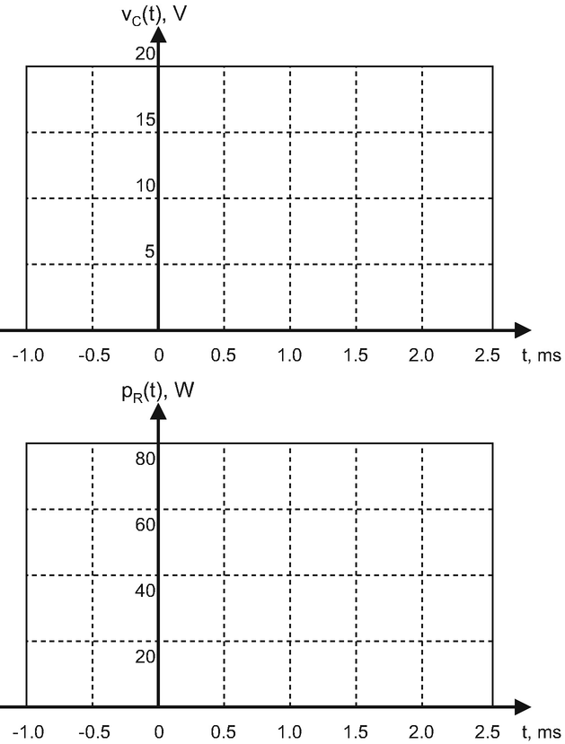
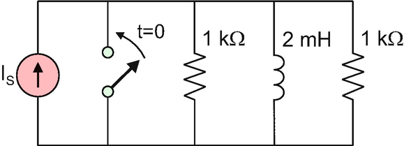
Problem 7.6
A 100-μF capacitor, shown in the following figure, discharges into a 10-Ω load resistor. The capacitor is charged to 15 V prior to \( t=0 \).
-
A.
Find the time constant of the circuit (show units).
-
B.
Express the voltage across the capacitor as a function of time and sketch it to scale versus time over time interval from −2 ms to 5 ms.


Problem 7.7
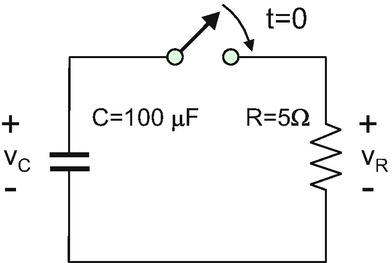
A 100-μF capacitor, shown in the following figure, discharges into a 5-Ω load resistor. The capacitor is charged to 20 V prior to \( t=0 \).
-
A.
Find an expression for the voltage across the capacitor as a function of time and sketch it to scale versus time over the interval from –2τ to 5τ.
-
B.
Repeat the exercise for instantaneous power delivered to the resistor.


Problem 7.8
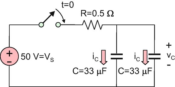
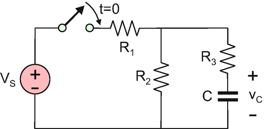
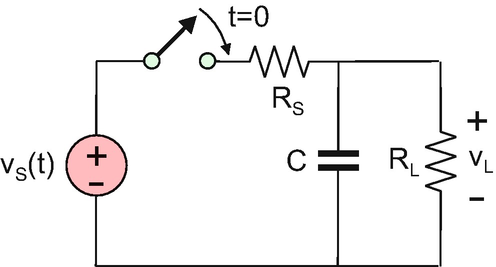
In the circuit shown in the following figure, the capacitor is charged to 20 V prior to \( t=0 \).
-
A.
Find an expression for the voltage across the capacitor as a function of time and sketch it to scale versus time over the interval from –2τ to 5τ.
-
B.
Repeat for instantaneous power delivered to the rightmost resistor.

Problem 7.9
Present the text of a MATLAB script (or of any software of your choice) in order to generate Fig. 7.2d of Section 7.1. Attach the figure so generated to the homework report.
Problem 7.10
Prove that the integral of the load power in Fig. 7.2d given by Eq.(7.8c) is exactly equal to the energy stored in the charged capacitor, \( {E}_{\mathrm{C}}=\frac{1}{2}C{V}_0^2 \) prior to \( t=0 \).
Problem 7.11
-
A.
Create the generic capacitor voltage discharge curve similar to Fig. 7.2a but for an arbitrary capacitor powering an arbitrary load resistor over the time interval from –2τ to 5τ. The capacitor is charged to V0 prior to \( t=0 \). To do so, find the capacitor voltage as a fraction of V0 for every unit of τ and fill out the Table that follows.
Capacitor voltage in terms of V0
t
−2τ
-τ
0
τ
2τ
3τ
4τ
5τ
υC(t)
-
B.
Repeat the same task for Fig. 7.2d related to load power. Find the load power in terms of the maximum power just after closing the switch.
Problem 7.12
For an unknown energy-release RC circuit, capacitor voltage and capacitor current were measured in laboratory before and after closing the switch at \( t=0 \) as shown in the figure that follows. Approximate R and C.

7.1.4 Application Example: Electromagnetic Railgun
7.1.5 Application Example: Electromagnetic Material Processing
Problem 7.13
An electromagnetic capacitor accelerator with permanent magnets has \( B=0.3\kern0.5em \mathrm{T} \). The accelerating object has a length of 2 cm. Plot to scale the Lorentz force as a function of discharge current over the interval \( 0<{i}_C<1000\kern0.5em \mathrm{A} \).
Problem 7.14
An electromagnetic capacitor accelerator needs to create an average force of 5 N over 2 ms on a moving object with length of 1 cm. The load (armature plus object) resistance is 1 Ω, and the external magnetic field is \( B=0.25\kern0.5em \mathrm{T} \). Determine:
-
A.
The required capacitor voltage prior to discharge
-
B.
The required capacitance of the capacitor (bank of capacitors)
Hint: Assume that the average force acts over the time interval τ. Its value is approximately equal to 60 % of the initial force value.
Problem 7.15
Solve the previous problem when:
-
A.
The average force increases to 50 N
-
B.
The average force increases to 500 N
Problem 7.16
The world's largest capacitor bank is located in Dresden, Germany. The pulsed, capacitive power supply system was designed and installed for studying high magnetic fields by experts from Rheinmetall Waffe Munition. The bank delivers 200 kA of discharge current in the initial time moment (just after the switch closes). The time constant is 100 ms. Estimate the bank capacitance if the charging voltage is 200 kV.

7.1.7 Energy-Accumulating Capacitor Circuit
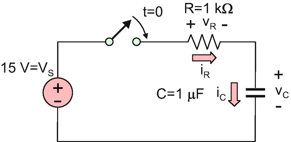
Problem 7.17
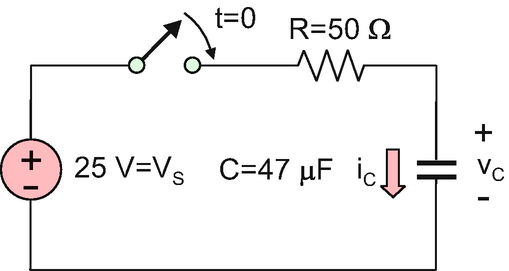
A 1-μF capacitor shown in the following figure is charged through the 1-kΩ load resistor. The initial capacitor voltage is zero.
-
A.
Find the time constant of the circuit (show units).
-
B.
Express the voltage across the capacitor as a function of time and sketch it to scale versus time over the interval from −2 ms to 5 ms.


Problem 7.18
For the circuit shown in the following figure:
-
A.
Find an expression for the capacitor voltage, υC, and the capacitor current, iC, including the value of time constant.
-
B.
Sketch the capacitor voltage, υC, and the capacitor current, iC, to scale versus time over the interval from –2τ to 5τ.

Problem 7.19
For the circuit shown in the following figure:
-
A.
Find an expression for the capacitor voltage, υC, and the capacitor current, iC, including the value of time constant.
-
B.
Sketch the capacitor voltage, υC, and the capacitor current, iC, to scale versus time over the time interval from –2τ to 5τ.

Problem 7.20
Sketch your own fluid-flow counterpart of the charging circuit shown in the figure and establish as many analogies between electrical (R, C, VS) and mechanical parameters of your drawing as possible.

Problem 7.21
For the circuit shown in the following figure:
-
A.
How much time does it take to charge the capacitor to 10 V?
-
B.
To 25 V?

Problem 7.22
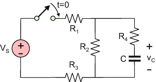
For the circuit shown in the figure, how much time does it take to charge the capacitor, C1, to 10 V? Assume that the initial voltages of both capacitors are zero.

Problem 7.23
For an unknown energy-accumulating RC circuit, capacitor voltage and capacitor current were measured in laboratory before and after closing the switch at \( t=0 \) as shown in the figure that follows. Approximate R and C.

Problem 7.24
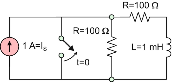
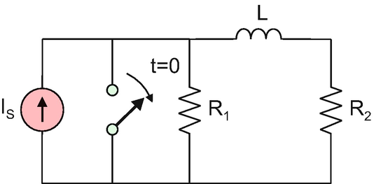
-
A.
Obtain an analytical solution for the capacitor voltage in the circuit shown in the following figure. When the switch is closed, the current source still generates current IS at its terminals. However, the supply is shorted out – no current flows into the circuit. When the switch is open, the current flows into the circuit.
-
B.
Could you convert this circuit to an equivalent RC transient circuit with the voltage source?
-
C.
Plot the voltage across the resistor versus time over the time interval from -2τ to 5τ.

Problem 7.25
Repeat the previous problem for the circuit shown in the following figure.

Problem 7.26
Obtain an analytical solution for the capacitor voltage in the circuit shown in the following figure at any time and express it in terms of Is, R1, R2, C. Find the time constant of the circuit when \( {R}_1={R}_2=100\kern0.5em \Omega, \kern0.5em C=47\kern0.5em \upmu \mathrm{F} \).

Problem 7.27
For the circuit shown in the figure:
-
A.
Derive and solve the dynamic circuit equation after the switch opens. Assume the initial capacitor voltage equal to zero.
-
B.
Plot the capacitor voltage to scale versus time over the time interval from –2τ to 5τ.

Problem 7.28
In the circuit that follows, the capacitor, C1, is initially uncharged. The switch is closed at \( t=0 \).

Give answers to the following questions based on known circuit parameters C1, R1, R2, VS:
-
A.
What is the current through resistor R2 as a function of time?
-
B.
What is the maximum current through resistor R1?
-
C.
What is the current through resistor R1 at a time long after the switch closes?
-
D.
What is the charge, \( {Q}^{+}(t) \), of the capacitor, C1, as a function of time?
The switch is then opened a very long time after it has been closed – reset the time to \( t=0 \).
-
A.
What is the charge \( {Q}^{+}(t) \) of the capacitor, C1, as a function of time?
-
B.
What is the current through resistor R2 as a function of time? Specify the current direction in the figure.
1.2 7.2 RL Circuits
7.2.1 Energy-Release Inductor Circuit
7.2.2 Continuity of the Inductor Current
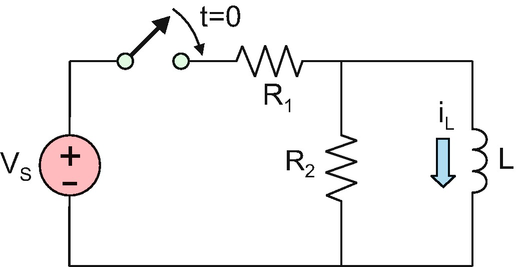
Problem 7.29
For the inductor as a dynamic circuit element, present:
-
1.
Equivalent circuit at DC
-
2.
Relation between voltage and current
-
3.
Expression for the time constant of a transient circuit that includes the dynamic element and a resistor, R
Dynamic circuit element |
|
Equivalent circuit at DC (short or open) | |
Relation between voltage and current (passive reference configuration) | |
Expression for the time constant of a transient circuit that includes the dynamic element (L) and a resistor R | \( \tau = \) |

Problem 7.30
-
A.
Using KCL and KVL, derive the differential equation for the inductor current in the circuit shown in the figure that follows, keeping the same labeling for the voltages and the currents.
-
B.
Is the final result different from Eq. (7.19) of Section 7.2?

Problem 7.31
Prove that Eq. (7.20) is the solution to Eq. (7.19) using direct substitution and the corresponding differentiation.
Problem 7.32
-
A.
Show that the time constant τ has units of seconds for the RL circuit.
-
B.
To ensure a slower energy release rate of the inductor, should the load resistance be small or large?
-
C.
To ensure a faster energy release rate of the inductor, should the load resistance be small or large?
Problem 7.33
A 6.8-μH inductor releases its energy into a load resistor as shown in the following figure. The load resistance may have values of 10 Ω, 100 Ω, and 1 kΩ. The inductor current is 1 A prior to \( t=0 \).

-
A.
Find time constant τ and the maximum instantaneous power delivered to the load resistor in the very first moment for every resistor value—fill out the Table that follows.
Instantaneous load power just after the switch closes
R
τ, s
\( {p}_{\mathrm{R}}\left(t=+0\right) \), W
10 Ω
100 Ω
1 kΩ
-
B.
Do those instantaneous power values from the Table depend on the inductance value?
Problem 7.34
Prove that the integral from 0 to ∞ of the load power in Fig. 7.10d is exactly equal to the energy stored in the inductor \( {E}_{\mathrm{L}}=\frac{1}{2}L{I}_{\mathrm{S}}^2 \) prior to \( t=0 \). Hint: The proof should include analytical integration of the instantaneous power in Eq. (7.21c).
Problem 7.35
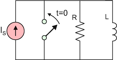
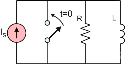
A 2-mH inductor, shown in the following figure, releases its energy into the 2-kΩ load resistor. The supply current is 0.8 A.
-
A.
Find the time constant of the RL circuit (show units).
-
B.
Express the current through the inductor as a function of time and sketch it to scale versus time over time interval from −2 μs to 5 μs.


Problem 7.36
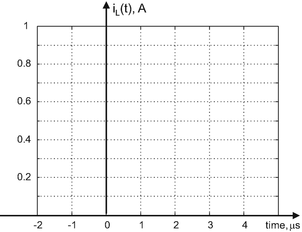
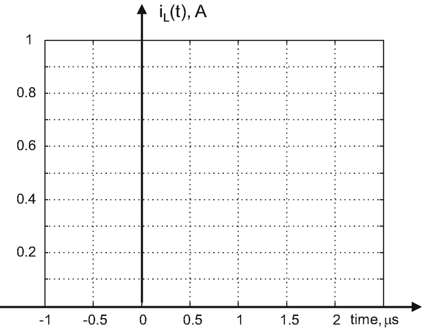
A 270-μH inductor, shown in the following figure, releases its energy into the 510-Ω load resistor. The supply current is 0.8 A.
-
A.
Find the time constant of the RL circuit (show units).
-
B.
Express the current through the inductor as a function of time and sketch it to scale versus time over time interval from −1 μs to 2.5 μs.
-
C.
Express the resistor voltage as a function of time and sketch it to scale versus time over time interval from −1 μs to 2.5 μs.


Problem 7.37
For an unknown energy-release RL circuit, inductor current and resistor voltage were measured before and after closing the switch at \( t=0 \) as shown in the figure that follows. Approximate R and L.

Problem 7.38
A 2-mH inductor, shown in the following figure, releases its energy into two 1-kΩ load resistors. The supply current is 100 mA.
-
A.
Find the time constant of the RL circuit (show units).
-
B.
Express the current through the inductor as a function of time and sketch it to scale versus time over time interval from −2 μs to 10 μs.


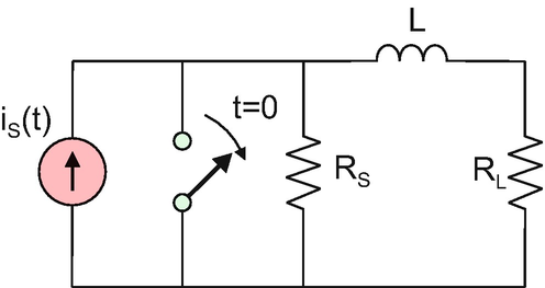
Problem 7.39
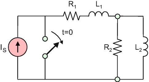
-
A.
Obtain the solution for the inductor current in the circuit shown in the figure at any time.
-
B.
Plot to scale the current through the inductor versus time over the interval from –2τ to 10τ.

7.2.3 Energy-Accumulating Inductor Circuit
Problem 7.40
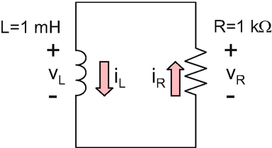
In the energy-accumulating RL circuit shown in the following figure, \( R=2\ \mathrm{k}\Omega \) and \( L=2\ \mathrm{mH} \). The supply current is 1 A.

-
A.
Find the time constant of the RL circuit (show units).
-
B.
Express the current through the inductor as a function of time and sketch it to scale versus time over time interval from −2 μs to 5 μs.


Problem 7.41
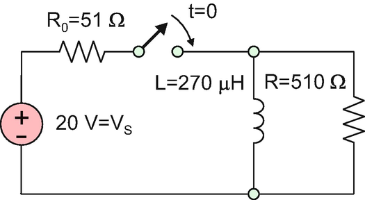
In the energy-accumulating RL circuit shown in the following figure, \( R=510\kern0.5em \Omega \) and \( L=270\kern0.5em \upmu \mathrm{H} \). The supply current is 1 A.
-
A.
Find the time constant of the RL circuit (show units).
-
B.
Express the current through the inductor as a function of time and sketch it to scale versus time over time interval from −1 μs to 2.5 μs.
-
C.
Express the resistor voltage as a function of time and sketch it to scale versus time over time interval from −1 μs to 2.5 μs.


Problem 7.42
-
A.
Obtain the solution for the inductor current in the circuit shown in the figure at any time.
-
B.
Plot the voltage across the rightmost resistor versus time over the interval from –2τ to 5τ.

7.2.4 Energy-Release RL Circuit with the Voltage Supply
7.2.5 Application Example: Laboratory Ignition Circuit
Problem 7.43
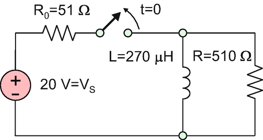
A 270-μH inductor shown in the following figure releases its energy into the 510-Ω load resistor. The power supply voltage is 20 V. The switch opens at \( t=0 \).
-
A.
Present an expression for the inductor current as a function of time and sketch it to scale versus time over the interval from −1 μs to 2.5 μs.
-
B.
Repeat the same task for the resistor voltage.

Problem 7.44
The circuit for the previous problem is converted to the energy-accumulating RL circuit by inversing the switch operation. Assume that the switch was open prior to \( t=0 \). The switch closes at \( t=0 \).
-
A.
Derive an expression for the inductor current as a function of time.
-
B.
Repeat the same task for the voltage across resistor R.
-
C.
Could this circuit generate large voltage spikes, similar to the circuit from the previous problem?

1.3 7.3 Switching RC Oscillator
7.3.2 Bistable Amplifier Circuit with the Positive Feedback
7.3.3 Triggering
Problem 7.45
The bistable amplifier circuit shown in the following figure (inverting Schmitt trigger) exists in the positive stable state. Amplifier’s power supply rails are ±12 V. Determine output voltage when the applied trigger signal is
-
1.
\( {\upsilon}_{\mathrm{in}}=6\kern0.5em \mathrm{V} \)
-
2.
\( {\upsilon}_{\mathrm{in}}=2\kern0.5em \mathrm{V} \)
-
3.
\( {\upsilon}_{\mathrm{in}}=-4\kern0.5em \mathrm{V} \)
Assume that the amplifier hits the power rails in saturation.

Problem 7.46
Repeat the previous problem when the initial stable state of the amplifier circuit is negative.
Problem 7.47
The bistable amplifier circuit shown in the following figure ( non-inverting Schmitt trigger) exists in the positive stable state. Amplifier’s power supply rails are ±15 V. Determine output voltage when the applied trigger signal is
-
A.
\( {\upsilon}_{\mathrm{in}}=-1\kern0.5em \mathrm{V} \)
-
B.
\( {\upsilon}_{\mathrm{in}}=-2\kern0.5em \mathrm{V} \)
-
C.
\( {\upsilon}_{\mathrm{in}}=-4\kern0.5em \mathrm{V} \)
Assume that the amplifier hits the power rails in saturation.

Problem 7.48
Repeat the previous problem when the initial stable state of the amplifier circuit is negative.
7.3.4 Switching RC Oscillator
7.3.5 Oscillation Frequency
Problem 7.49
A clock circuit (relaxation oscillator circuit) shown in the following figure is powered by a ±10-V power supply.

Sketch to scale the capacitor voltage, υC, as a function of time. Assume that \( {\upsilon}_{\mathrm{C}}\left(t=0\right)=0 \). Assume the ideal amplifier model. The specific values of R and C do not matter; they are already included in the time scale.
Problem 7.50
An RC clock circuit is needed with the oscillation frequency of 1 kHz and amplitude of the capacitor voltage of 4 V. Determine one possible set of circuit parameters R1, R2, R given that the capacitance of 100 nF is used. The power supply voltage of the amplifier is ±12 V. Assume that the amplifier hits the power rails in saturation.
Problem 7.51
A relaxation oscillator circuit may generate nearly triangular waveforms at the capacitor. Which values should the feedback factor \( \beta =\frac{R_1}{R_1+{R}_2} \) attain to make it possible?
1.4 7.4 Single-Time-Constant (STC) Transient Circuits
7.4.1 Circuits with Resistances and Capacitances
7.4.2 Circuits with Resistances and Inductances
Problem 7.52
Determine whether or not the transient circuits shown in the following figure are the STC circuits. If this is the case, express the corresponding time constant in terms of the circuit parameters.

Problem 7.53
Repeat the previous problem for the circuits shown in the following figure.

7.4.3 Example of a Non-STC Transient Circuit
Problem 7.54
Using software of your choice, generate the solution for the non-STC circuit in Fig. 7.25a over the time interval from 0 to 15τ0 where \( {\tau}_0= RC \) with \( {C}_1={C}_2=C \), \( {R}_1={R}_2=R \). Use \( R=1\kern0.5em \mathrm{k}\Omega \), \( C=1\kern0.5em \upmu \mathrm{F} \), and \( {V}_{\mathrm{S}}=10\kern0.5em \mathrm{V} \). Plot two capacitor voltages and the circuit current as functions of time to scale.
Problem 7.55
-
A.
Derive the general ODE for the non-STC circuit in Fig. 7.25a in terms of υ1 for arbitrary circuit parameters.
-
B.
Present its particular form when \( {C}_1={C}_2=C \) and \( {R}_1=2{R}_2=R \). Express all coefficients in terms of \( {\tau}_0= RC \).
-
C.
Given that the solution for the homogeneous ODE has the form \( \exp \left(-\alpha \kern0.1em t/{\tau}_0\right) \), determine two possible solutions for the dimensionless coefficient α.
-
D.
Using software of your choice, generate the circuit solution over the time interval from 0 to 15τ0. Use \( R=1\kern0.5em \mathrm{k}\Omega \), \( C=1\kern0.5em \upmu \mathrm{F} \), and \( {V}_{\mathrm{S}}=10\kern0.5em \mathrm{V} \). Plot two capacitor voltages and the circuit current as functions of time to scale.

7.4.4 Example of a STC Circuit
Problem 7.56
For the circuit shown in Fig. 7.26, derive ODEs for inductor currents i1, i2.
7.4.5 Method of Thévenin Equivalent. Application Example: Circuit with a Bypass Capacitor
Problem 7.57
In the circuit from Fig. 7.27a, another resistance R0 is present in series with the capacitance C. Determine the natural response of the circuit and find the corresponding time constant, τ.
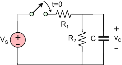
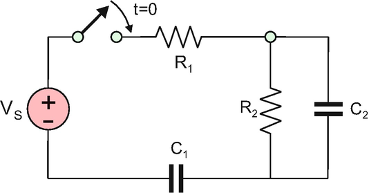
Problem 7.58
A transient circuit with the DC voltage source VS is shown in the following figure. Given that \( {V}_S=10\kern0.5em \mathrm{V} \) and \( {R}_1=1\kern0.5em \mathrm{k}\Omega \), \( {R}_2=1\kern0.5em \mathrm{k}\Omega \), and \( C=1\kern0.5em \upmu \mathrm{F} \):
-
A.
Present the ODE for the capacitor voltage υC(t).
-
B.
Determine the value of the time constant τ and the ODE right-hand side (the forcing function).
-
C.
Present the solution for the capacitor voltage as a function of time assuming an initially uncharged capacitor

Problem 7.59
A transient circuit with the DC voltage source VS is shown in the following figure. Given that \( {V}_{\mathrm{S}}=10\kern0.5em \mathrm{V} \) and \( {R}_1={R}_2=1\kern0.5em \mathrm{k}\Omega \), \( {R}_3=2\kern0.5em \mathrm{k}\Omega \), and \( C=1\kern0.5em \upmu \mathrm{F} \):
-
A.
Present the ODE for the capacitor voltage υC(t).
-
B.
Determine the value of the time constant τ and the ODE right-hand side (the forcing function).
-
C.
Present the solution for the capacitor voltage as a function of time assuming an initially uncharged capacitor.

Problem 7.60
A transient circuit with the DC voltage source VS is shown in the following figure. Given that \( {V}_{\mathrm{S}}=10\ \mathrm{V} \) and\( {R}_1={R}_2=1\ \mathrm{k}\Omega \), \( {R}_3={R}_4=2\kern0.5em \mathrm{k}\Omega \), and \( C=1\kern0.5em \upmu \mathrm{F} \):
-
A.
Present the ODE for the capacitor voltage υC(t).
-
B.
Determine the value of the time constant τ and the ODE right-hand side (the forcing function).
-
C.
Present the solution for the capacitor voltage as a function of time assuming an initially uncharged capacitor.

Problem 7.61
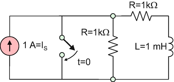
A transient circuit with the current source IS is shown in the following figure. Given that \( {I}_{\mathrm{S}}=10\kern0.5em \mathrm{mA} \) and \( {R}_1={R}_2=1\kern0.5em \mathrm{k}\Omega \) and \( L=1\kern0.5em \mathrm{mH} \):
-
A.
Present the ODE for the inductor current iL(t).
-
B.
Determine the value of the time constant τ and the ODE right-hand side (the forcing function).
-
C.
Present the solution for the inductor current as a function of time assuming the initial current equal to zero.

Problem 7.62
A transient circuit with the DC voltage source VS is shown in the figure below. Given that \( {V}_{\mathrm{S}}=10\kern0.5em \mathrm{V} \) and \( {R}_1={R}_2=1\kern0.5em \mathrm{k}\Omega, L=1\kern0.5em \mathrm{mH} \):
-
A.
Present the ODE for the inductor current iL(t).
-
B.
Determine the value of the time constant τ and the ODE right-hand side (the forcing function).
-
C.
Present the solution for the inductor current as a function of time assuming the initial current equal to zero.

Problem 7.63
Consider the circuits in two previous problems at arbitrary values of R1, R2, L, IS, VS. What should be the relation between these parameters to guarantee the same solution for the inductor current in every case?
Problem 7.64
Describe the mathematical meaning of
-
A.
Natural response
-
B.
Forced response
for a first-order transient circuit in your own words. Do you think that this concept can be applied to any transient circuit?
Problem 7.65
If a transient circuit uses a DC supply (either voltage or current) and a switch, what is a general form of the forcing function?
Problem 7.66
If the forcing function of a first-order transient circuit is a combination of sine/cosine function and a constant, what is the general form of the forced response?
Problem 7.67
In the transient circuit shown in the figure below, \( {\upsilon}_{\mathrm{S}}(t)={V}_{\mathrm{S}}+{V}_{\mathrm{m}}\sin \omega \kern0.1em t \).
-
A.
Write the solution for the voltage across the load resistor RL in terms of the circuit parameters assuming an initially uncharged capacitor.
-
B.
Write the solution for the voltage across the load resistor RL when the bypass capacitor is absent.

Problem 7.68
Plot to scale the load voltage for the circuit shown in Fig. 7.27a with and without the bypass capacitor over time interval from 0 to 50 ms. The circuit parameters are \( {R}_S=5\kern0.5em \Omega, {R}_L=1\kern0.5em \mathrm{k}\Omega, \kern0.5em C=500\kern0.5em \upmu \mathrm{F} \). The source given by Eq. (7.50) is the superposition of the DC and AC components. The source parameters are \( {V}_{\mathrm{S}}=10\kern0.5em \mathrm{V},\kern0.5em {V}_{\mathrm{m}}=1\mathrm{V},\kern0.5em f=250\kern0.6em \mathrm{Hz} \).
Problem 7.69
What is the asymptotic form of the solution given by Eqs. (7.57)–(7.58) when the source resistance, RS, tends to zero?
Problem 7.70
In the transient circuit shown in the figure below, assume \( {i}_{\mathrm{S}}(t)={I}_{\mathrm{S}}+{I}_{\mathrm{m}}\sin \omega \kern0.1em t \).
-
A.
Write the solution for the current through the load resistor RL in terms of the circuit parameters assuming that the initial inductor current is equal to zero.
-
B.
Write the solution for the current through the load resistor RL when the decoupling inductor is absent

Problem 7.71
In the circuit for the previous problem, another resistor R0 is present in parallel with the inductance L. Determine the natural response of the circuit and find the time constant, τ.
1.5 7.5 Description of the Second-Order Transient Circuits
7.5.1 First-order Transient Circuits Versus Second-order Transient Circuits
Problem 7.72
A transient circuit is shown in the following figure. Is it a first- or second-order transient circuit? Justify your answer.

Problem 7.73
A transient circuit is shown in the figure below. Is it a first- or second-order transient circuit? Justify your answer.

Problem 7.74
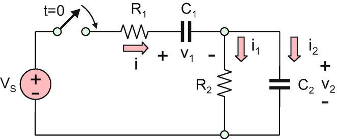
Establish the ODE for the transient circuit shown in the figure below. Both capacitors have zero voltage prior to closing the switch.
-
A.
Assume \( {R}_1={R}_2=R,{C}_1={C}_2=C \).
-
B.
Assume arbitrary values of R1,2, C1,2.

Problem 7.75
Establish the ODE for the transient circuit shown in the figure below. Inductor currents are zero prior opening the switch.
-
A.
Assume \( {R}_1={R}_2=R,{L}_1={L}_2=L \).
-
B.
Assume arbitrary values of R1,2, L1,2.

Problem 7.76
In the previous problem, add resistance R3 as shown in the figure that follows and solve task B.

7.5.2 Series Connected Second-order RLC Circuit
Problem 7.77
Describe in your own words the mechanical counterpart of the series RLC circuit.
Problem 7.78
An RLC circuit in Fig. 7.30 has \( R=1\kern0.5em \mathrm{k}\Omega, \kern0.5em C=1\kern0.5em \upmu \mathrm{F},L=1\kern0.5em \mathrm{mH} \).
-
A.
Find the value of the damping coefficient, α (show units).
-
B.
Find the value of undamped resonant frequency, ω0.
Problem 7.79
How does the second-order ODE Eq. (7.63) for the circuit current in the series RLC circuit from Fig. 7.30 change if the capacitor was charged to VS/2 prior to \( t=0 \)?
Problem 7.80
In the circuit shown in Fig. 7.30, the switch is replaced by a short circuit. The constant voltage source is replaced by an arbitrary time-varying voltage source \( {V}_{\mathrm{S}}\to {\upsilon}_{\mathrm{S}}(t) \) as shown in the figure that follows. Derive the dynamic circuit equation for the circuit current similar to Eq. (7.63) of this section. Present your result in terms of damping coefficient α and undamped resonant frequency ω0.

7.5.3 Choice of Independent Function: Initial Conditions
7.5.4 Step Response
Problem 7.81
The RLC circuit shown in Fig. 7.30 is described by dynamic equation (7.63) written in terms of the electric current. How do the initial conditions to this equation change if the capacitor was charged to VS/2 prior to \( t=0 \)?
Problem 7.82
For the circuit shown in Fig. 7.30:
-
A.
Derive the dynamic circuit equation (7.67) in terms of the capacitor voltage υC(t).
-
B.
How does this equation change if the capacitor was charged to VS/2 prior to \( t=0 \)?
Problem 7.83
For the series RLC circuit with the switch and the DC supply shown in Fig. 7.30, we know the solution, υC(t), of Eq. (7.67) or Eq. (7.69) for \( {V}_{\mathrm{S}}=1\kern0.5em \mathrm{V} \). The circuit shown in the following figure is now considered, with the voltage source in the form of a voltage pulse (one bit) centered about \( t=0 \). Express the solution to the present problem in terms of υC(t).

Problem 7.84
Repeat the previous problem for the voltage source shown in the figure that follows (a voltage pulse train of two bits).

Problem 7.85
Repeat Problem 7.83 for the voltage source shown in the figure that follows (a bipolar voltage pulse).

7.5.5 Parallel Connected Second-Order RLC Circuit
Problem 7.86
For the circuit shown in Fig. 7.34:
-
A.
Derive the dynamic circuit equation (7.75) written in terms of the inductor current iL(t).
-
B.
How does this equation change if the switch in Fig. 7.34 was open prior to \( t=0 \) and closes at \( t=0 \)?
-
C.
How do the initial conditions change in this case?
Problem 7.87
Describe the duality between series and parallel RLC circuits in your own words.
Problem 7.88
For the parallel RLC circuit with the switch and the DC current source shown in Fig. 7.34, we know the solution, iL(t), of Eq. (7.75) for \( {I}_{\mathrm{S}}=1\kern0.5em \mathrm{mA} \). The circuit shown in the following figure is now considered, with the current source in the form of a pulse (one bit) centered about \( t=0 \). Express the solution to in terms of iL(t).

1.6 7.6. Step Response of the Series RLC Circuit
7.6.1 General Solution of the Second-order ODE
7.6.2 Derivation of Complementary Solution
Problem 7.89
-
A.
The complete solution to a second-order homogeneous ODE is a sum of two distinct components. Describe each of them.
-
B.
Write three forms of the complementary solution (natural response) for the second-order homogeneous ODE.
-
C.
What is a new parameter to be introduced for the underdamped circuit?
Problem 7.90
For the series RLC circuit shown in the following figure:
-
A.
Find the value of the damping coefficient, α (show units).
-
B.
Find the value of the undamped resonant frequency, ω0 (show units).
-
C.
Find the value of the damping ratio, ζ (show units).
-
D.
Find the particular solution (forced response).
-
E.
Outline the form of the complementary solution (natural response).
-
F.
Which value should the circuit resistance have for a critically damped circuit?

Problem 7.91
Repeat the previous problem for the series RLC circuit shown in the figure below.

Problem 7.92
For the series RLC circuit shown in the following figure, fill out the table of circuit parameters.

Table of circuit parameters
R, Ω | ζ | Circuit type (overdamped, critically damped, underdamped) |
25 | ||
50 | ||
75 | ||
100 |
Given fixed L and C, which values of resistance (large or small) lead to the overdamped circuit?
Problem 7.93
For the series RLC circuit shown in the figure below, fill out the table of circuit parameters.

Table of circuit parameters
C, μF | ζ | Circuit type (overdamped, critically damped, underdamped) |
0.01 | ||
0.1 | ||
0.4 | ||
1.0 |
Given fixed L and R, which values of capacitance (large or small) lead to the overdamped circuit?
Problem 7.94
For the series RLC circuit shown in the following figure, fill out the table of circuit parameters.

Table of circuit parameters
L, μH | ζ | Circuit type (overdamped, critically damped, underdamped) |
0.1 | ||
1 | ||
2.5 | ||
10 |
Given fixed R and C, which values of inductance (large or small) lead to the overdamped circuit?
Problem 7.95
Show that underdamped solution and critically damped solutions coincide with each other when \( \varsigma \to 1 \).
7.6.3 Finding Integration Constants
7.6.4 Solution Behavior for Different Damping Ratios
Problem 7.96
For the circuit shown in the figure below:

-
A.
Determine damping coefficient α, undamped resonant frequency ω0, and damping ratio ζ.
-
B.
Determine constants K1, K2.
-
C.
Write solution for the capacitor voltage with all constants defined.
-
D.
Calculate and plot to scale capacitor voltage at 0, 0.05, 0.1, 0.2, and 0.3 μs.
Problem 7.97
For the circuit shown in the following figure:
-
A.
Determine damping coefficient α, undamped resonant frequency ω0, and damping ratio ζ.
-
B.
Determine constants K1, K2.
-
C.
Write the solution for the capacitor voltage with all constants defined.
-
D.
Calculate capacitor voltage at 0, 1, 2, 3, 4, and 5 ms and plot it to scale versus time.

Problem 7.98
Repeat the previous problem for the circuit shown in the following figure.

Problem 7.99
In the circuit shown in the figure below, the capacitor was charged to 10 V prior to closing the switch.

-
A.
How are the circuit equation and initial conditions different from Eqs. (7.78a, b)?
-
B.
Determine damping coefficient α, undamped resonant frequency ω0, and damping ratio ζ.
-
C.
Determine constants K1, K2.
-
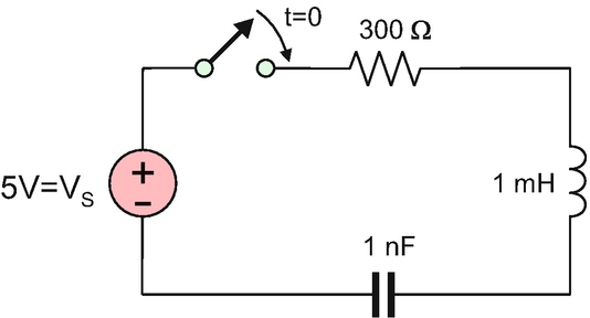
D.
Write the solution for capacitor voltage with all constants defined.
-
E.
Calculate the capacitor voltage at 0, 1, 2, 3, 4, and 5 ms and plot it to scale versus time.
7.6.5 Overshoot and Rise Time
7.6.6 Application: Non-ideal Digital Waveform
Problem 7.100
The following figure shows the underdamped step response for a series RLC circuit. The DC source has the voltage of 10 V. Using the figure:
-
A.
Estimate the overshoot percentage.
-
B.
Estimate the rise time.
-
C.
Do these estimates (approximately) agree with Eqs. (7.88a, b)?

Problem 7.101
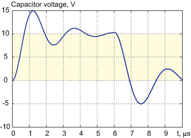
Capacitor voltage is measured in a series RLC circuit as shown in the figure to the previous problem. Given \( R=2\;\Omega \), estimate circuit inductance L and circuit capacitance C.
Problem 7.102
The figure that follows shows the distorted rectangular waveform (capacitor voltage) for the circuit shown in Fig. 7.33. The DC source has the voltage of 10 V.
-
A.
Using the figure, estimate the overshoot and undershoot percentages.
-
B.
Using the figure, estimate the rise time and the fall time.
-
C.
Do these estimates (approximately) agree with Eqs. (7.88a, 7.88b)?

Problem 7.103
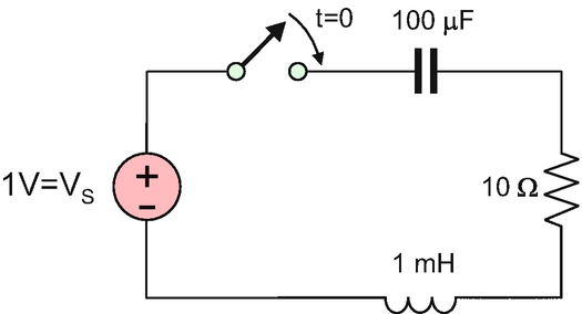
For the circuit shown in the following figure:

-
A.
Determine the step response υC(t) for the circuit shown in figure (a) given that \( L=1\kern0.5em \upmu \mathrm{H},\kern0.5em C=1\kern0.5em \mathrm{nF}, \) \( {V}_{\mathrm{S}}=10\kern0.5em \mathrm{V} \), and \( R=75\kern0.5em \Omega \).
-
B.
Express the solution υ pulseC (t) for the voltage pulse shown in figure (b) in terms of the step response.
-
C.
Given \( T=0.5\kern0.5em \upmu \mathrm{s} \), calculate the solution for the voltage pulse over the time interval from 0 to 0.7 μs in steps of 0.1 μs and plot it to scale.
Problem 7.104
Repeat the previous problem assuming \( T=0.2\kern0.5em \upmu \mathrm{s} \). Calculate the solution for the voltage pulse over the time interval from 0 to 0.5 μs in steps of 0.05 μs and plot it to scale versus time.
Rights and permissions
Copyright information
© 2019 Springer Nature Switzerland AG
About this chapter

Cite this chapter
Makarov, S.N., Ludwig, R., Bitar, S.J. (2019). Transient Circuit Fundamentals. In: Practical Electrical Engineering. Springer, Cham. https://doi.org/10.1007/978-3-319-96692-2_7
Download citation
DOI: https://doi.org/10.1007/978-3-319-96692-2_7
Published:
Publisher Name: Springer, Cham
Print ISBN: 978-3-319-96691-5
Online ISBN: 978-3-319-96692-2
eBook Packages: EngineeringEngineering (R0)