
Abstract
Knowledge of major circuit elements (dependent sources) and theirυ-i characteristics (Chap.2)
Access this chapter
Tax calculation will be finalised at checkout
Purchases are for personal use only
Author information
Authors and Affiliations
Appendices
Summary
Amplifier circuit | Operation | Formulas |
Open-loop operational amplifier (comparator)
|
| Operation with\( \pm {V}_{\mathrm{CC}} \) power rails: \( {\upsilon}_{\mathrm{out}}=A\left({\upsilon}^{+}-{\upsilon}^{-}\right),\kern1em \left|{\upsilon}_{\mathrm{out}}\right|<{V}_{\mathrm{CC}} \) Open-circuit (open-loop) gainA is very high |
Amplifier circuit model
|
| – Valid forany voltage amplifier or voltage amplifier circuit, butR in,R out,A are different in every case; – Ideal amplifier model (useful simplification): \( {R}_{\mathrm{in}}=\infty \),\( {R}_{\mathrm{out}}=0 \),\( A=\infty \) |
Negative feedback for the ideal-amplifier model: differential input voltage is zero (2nd SPC) | ||
Non-inverting amplifier
|
| For ideal-amplifier model: \( {\upsilon}_{\mathrm{out}}={A}_{\mathrm{CL}}{\upsilon}_{\mathrm{in}},\kern0.5em {A}_{\mathrm{CL}}=1+\frac{R_2}{R_1} \) \( {R}_{\mathrm{in}}=\infty \),\( {R}_{\mathrm{out}}=0 \) Exact:\( {A}_{\mathrm{CL}}=A{\left(1+A\frac{R_1}{R_1+{R}_2}\right)}^{-1} \) |
Voltage follower (buffer) amplifier
|
| For ideal-amplifier model: \( {\upsilon}_{\mathrm{out}}={A}_{\mathrm{CL}}{\upsilon}_{\mathrm{in}},\kern0.5em {A}_{\mathrm{CL}}=1 \) \( {R}_{\mathrm{in}}=\infty \),\( {R}_{\mathrm{out}}=0 \) Exact:\( {A}_{\mathrm{CL}}=\frac{A}{1+A} \) |
Inverting amplifier
|
| For ideal-amplifier model: \( {\upsilon}_{\mathrm{out}}={A}_{\mathrm{CL}}{\upsilon}_{\mathrm{in}},\kern0.5em {A}_{\mathrm{CL}}=-\frac{R_2}{R_1} \) \( {R}_{\mathrm{in}}={R}_1 \),\( {R}_{\mathrm{out}}=0 \) Exact:\( {A}_{\mathrm{CL}}=-\frac{R_2}{R_1}A{\left(A+1+\frac{R_2}{R_1}\right)}^{-1} \) |
Cascaded amplifier
|
| – Gains of individual stages multiply; – Input resistance of the amplifier circuit is the input resistance of stage 1; – Individual stage gain should not exceed 100 |
Input load bridging versus input load matching | ||
Load bridging
|
| – Source (sensor) sees the amplifier as an open circuit: \( {\upsilon}_{\mathrm{out}}={\upsilon}_{\mathrm{S}}\times {A}_{\mathrm{CL}} \) – No current from the source can flow into amplifier circuit |
Load matching
|
| – Source (sensor) sees the amplifier as resistance\( {R}_{\mathrm{in}}={R}_1 \): \( {\upsilon}_{\mathrm{out}}=\frac{R_{\mathrm{in}}}{R_{\mathrm{S}}+{R}_{\mathrm{in}}}{\upsilon}_{\mathrm{S}}\times {A}_{\mathrm{CL}} \) – Matching condition\( {R}_{\mathrm{S}}={R}_{\mathrm{in}} \) is important for high-freq. circuits |
DC imperfections and their cancellation | ||
Non-inverting amplifier
|
| – Short-circuited output voltage may be trimmed to zero using the offset null terminal – Short-circuited output voltage may be trimmed to zero by adjusting common-terminal voltage; – Extra resistanceR eliminates the effect of the input bias current |
Inverting amplifier
|
| The same as above |
Multiple-input amplifier circuits | ||
Summing amplifier
|
| – The summing amplifier sums several weighted input voltages: \( {\upsilon}_{\mathrm{out}}=-\frac{R_{\mathrm{F}}}{R_1}{\upsilon}_1-\frac{R_{\mathrm{F}}}{R_2}{\upsilon}_2-\frac{R_{\mathrm{F}}}{R_3}{\upsilon}_3 \) – Used as a prototype of the digital to analog converter |
Difference amplifier
|
| – True difference amplifier: \( \frac{R_2}{R_1}=\frac{R_4}{R_3} \),\( {\upsilon}_{\mathrm{out}}=\frac{R_2}{R_1}\left({\upsilon}_a-{\upsilon}_b\right) \) – Rejects common-mode voltage – For the general difference amplifier circuit see Eq. (5.52c) |
Unity common-mode gain stage
|
| – Differential gain: \( {\upsilon}_a*-{\upsilon}_b*={A}_{\mathrm{D}}\left({\upsilon}_a-{\upsilon}_b\right) \) \( {A}_{\mathrm{D}}=1+\frac{R_4}{R_3} \) – Common-mode gain: \( {\upsilon}_a*+{\upsilon}_b*={A}_{\mathrm{CM}}\left({\upsilon}_a+{\upsilon}_b\right) \) \( {A}_{\mathrm{CM}}=1 \) |
Instrumentation amplifier
|
| Output voltage: \( {\upsilon}_{\mathrm{out}}=\frac{R_2}{R_1}\left(1+\frac{R_4}{R_3}\right)\left({\upsilon}_a-{\upsilon}_b\right) \) Closed-loop differential gain: \( {A}_{\mathrm{CL}}=\frac{R_2}{R_1}\left(1+\frac{R_4}{R_3}\right) \) – Rejects common-mode voltage |
Simpler instrumentation amplifier
|
| Output voltage: \( {\upsilon}_{\mathrm{out}}=\left(2\frac{R_2}{R_{\mathrm{G}}}+\left(1+\frac{R_2}{R_1}\right)\right)\left({\upsilon}_a-{\upsilon}_b\right) \) – Closed-loop differential gain: \( {A}_{\mathrm{CL}}=2\frac{R_2}{R_{\mathrm{G}}}+\left(1+\frac{R_2}{R_1}\right) \) – Rejects common-mode voltage |
General feedback systems and amplifiers with negative feedback | ||
Signal—flow diagram
|
| Closed-loop gain: \( {x}_{\mathrm{out}}={A}_{\mathrm{CL}}{x}_{\mathrm{in}},\kern0.5em {A}_{\mathrm{CL}}=\frac{A}{1+A\beta}\approx \frac{1}{\beta } \) Error signal: \( {x}_e=\frac{1}{1+A\beta }{x}_{\mathrm{in}}\approx 0 \) |
Transconductance amplifier
|
| Closed-loop operation: \( {i}_{\mathrm{out}}={G}_{\mathrm{F}}{\upsilon}_{\mathrm{in}},\kern0.5em {G}_{\mathrm{F}}=1/{R}_{\mathrm{F}} \) Variations of this simple circuit are possible |
Transresistance amplifier
|
| Closed-loop operation: \( {\upsilon}_{\mathrm{out}}=-{R}_{\mathrm{F}}{i}_{\mathrm{in}} \) Variations of this simple circuit are possible |
Current amplifier
|
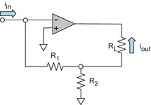
| Closed-loop operation: \( {i}_{\mathrm{out}}=\left(1+\frac{R_2}{R_1}\right){i}_{\mathrm{in}} \) Variations of this simple circuit are possible |
Howland amplifier (current pump)
|
| Closed-loop operation: (\( {R}_1/{R}_3={R}_2/{R}_4 \)) \( {i}_{\mathrm{out}}={G}_{\mathrm{F}}\left({\upsilon}_a-{\upsilon}_b\right),\kern0.5em {G}_{\mathrm{F}}=1/{R}_2 \) Variations of this clever circuit are possible |


Problems
2.1 5.1 Amplifier operation and circuit models
5.1.1 Amplifier Operation
Problem 5.1
An operational amplifier has five terminals.
-
A.
Sketch the amplifier symbol.
-
B.
Name each of the op-amp terminals and describe its function in one sentence per terminal.
-
C.
Can the amplifier IC have more than five terminals? Explain.
Problem 5.2
You may wonder about the meaning of the two letters preceding amplifier marking, e.g., LM741. Each of the semiconductor companies has its own abbreviation, e.g., LM for an amplifier designed and manufactured by the National Semiconductor Corporation (acquired by Texas Instruments in 2011), AD for an amplifier manufactured by Analog Devices, MC for STMicroelectronics, TL for Texas Instruments, etc. The same chip, e.g., LM741, may be manufactured by several semiconductor chip makers. The part number is given by a numerical code that is imprinted on the top of the package. An MC1458 amplifier IC chip is shown in the figure below. This IC is adual operational amplifier. In other words, one such IC package contains two separate operational amplifiers.

-
A.
Download the amplifier’s datasheet fromhttp://www.datasheetcatalog.com
-
B.
Redraw the figure to this problem in your notes and label the pins for the non-inverting input, the inverting input, and the output of the operational amplifier #1.
-
C.
Label pins for\( +{V}_{\mathrm{CC}} \) and\( -{V}_{\mathrm{CC}} \).
Problem 5.3
What is the minimum number of pins required for:
-
A.
The dual operational amplifier (the corresponding IC package contains two separate operational amplifiers)?
-
B.
Thequad operational amplifier (the corresponding IC package contains four separate operational amplifiers)?
Problem 5.4
An operational amplifier has an open-circuit gain of\( A=2\times {10}^5 \) and is powered by a dual source of ±10 V. It is operated in the open-circuit configuration. What is the amplifier’s open-circuit output voltageυ out if
-
A.
\( {\upsilon}^{+}=0\mathrm{V},\kern0.5em {\upsilon}^{-}=0\mathrm{V} \)
-
B.
\( {\upsilon}^{+}=+1\mathrm{V},\kern0.5em {\upsilon}^{-}=+1\mathrm{V} \)
-
C.
\( {\upsilon}^{+}=+1\mathrm{V},\kern0.5em {\upsilon}^{-}=0\mathrm{V} \)
-
D.
\( {\upsilon}^{+}=0\mathrm{V},\kern0.5em {\upsilon}^{-}=-1\mathrm{V} \)
-
E.
\( {\upsilon}^{+}=+1\mathrm{mV},\kern0.5em {\upsilon}^{-}=0\mathrm{V} \)
-
F.
\( {\upsilon}^{+}=-1\mathrm{mV},\kern0.5em {\upsilon}^{-}=0\mathrm{V} \)
-
G.
\( {\upsilon}^{+}=10\mu \mathrm{V},\kern0.5em {\upsilon}^{-}=0\mathrm{V} \)
-
H.
\( {\upsilon}^{+}=0\mathrm{V},\kern0.5em {\upsilon}^{-}=10\mu \mathrm{V} \)
Problem 5.5
Based on the solution to Problem5.4, why do you think the operational amplifier is seldom used in the open-loop configuration, at least in analog electronics?
Problem 5.6
Using the website of the National Semiconductor Corporation, determine the maximum and minimum supply voltages (operating with the dual-polarity power supply) for the following amplifier’s ICs:
-
A.
LM358
-
B.
LM1458
-
C.
LM741
Which amplifier IC from the list may be powered by two AAA batteries?
Problem 5.7
Plot to scale the output voltage of the operation amplifier with an open-circuit gain\( A=5\times {10}^4 \) when the non-inverting input voltage\( {\upsilon}^{+} \) changes from −2 mV to +2 mV and the inverting input voltage\( {\upsilon}^{-} \) is equal to −1 mV. The amplifier is powered by a ±12-V dual voltage supply. Label the axes.
Problem 5.8
Repeat the previous problem for\( A=5\times {10}^5 \).
5.1.2 Operational Amplifier Comparator
Problem 5.9
In a circuit shown in the figure below, an operational amplifier is driven by a ±10-V dual power supply (not shown). The open-circuit DC gain of the amplifier is\( A=1,000,000 \). Sketch to scale the output voltage to the amplifier when
-
a)
\( {V}_{\mathrm{threshold}}=-30\kern0.5em \mathrm{mV} \)
-
b)
\( {V}_{\mathrm{threshold}}=+30\kern0.5em \mathrm{mV} \)
Assume that the amplifier hits the power rails in saturation.

Problem 5.10
Based on the solution to the previous problem, why do you think the operational amplifier in the open-loop configuration may be useful for digital circuits?
Problem 5.11
Solve Problem5.9 when the input voltage is applied to the inverting input and the threshold voltage is applied to the non-inverting input.
Problem 5.12
The circuit shown in the figureis azero-level detector. An operational amplifier in the open-loop configuration is driven by a ±10-V dual power supply (not shown). The open-circuit amplifier gain is 100,000. Sketch the output voltage to scale. Assume that the amplifier hits the power rails in saturation.

Problem 5.13
In a circuit shown in the figure below, an operational amplifier is driven by a ±15-V dual power supply (not shown). The open-circuit gain of the amplifier is\( A=100,000 \). Sketch to scale the output voltage to the amplifier when
-
a)
\( {V}_{\mathrm{threshold}}=0\kern0.5em \mathrm{mV} \)
-
b)
\( {V}_{\mathrm{threshold}}=+4\kern0.5em \mathrm{mV} \)
Assume that the amplifier hits the power rails in saturation.

5.1.3 Amplifier Circuit Model
5.1.4 Ideal-Amplifier Model
Problem 5.14
-
A.
Draw the circuit model of an operational amplifier.
-
B.
Describe the meaning of the amplifier as the voltage-controlled voltage source in your own words.
Problem 5.15
For an equivalent amplifier circuit with\( A=1500 \) shown in the figure below, determine the output voltage given that\( {\upsilon}_{\mathrm{S}}(t)=1 \cos \omega \kern0.1em t\kern0.5em \left[\mathrm{mV}\right] \),\( {R}_{\mathrm{S}}=50\kern0.5em \Omega \),\( {R}_{\mathrm{L}}=50\kern0.5em \Omega \) for three cases:
-
A.
\( {R}_{\mathrm{in}}=100\kern0.5em \mathrm{k}\Omega \) and\( {R}_{\mathrm{out}}=2\kern0.5em \Omega \).
-
B.
\( {R}_{\mathrm{in}}=50\kern0.5em \Omega \) and\( {R}_{\mathrm{out}}=25\kern0.5em \Omega \).
-
C.
\( {R}_{\mathrm{in}}=\infty \) and\( {R}_{\mathrm{out}}=0 \).

Problem 5.16
Name one reason why we should attempt to:
-
A.
Make the input resistance (impedance) to the amplifier as high as possible.
-
B.
Make the output resistance (impedance) to the amplifier as low as possible.
Problem 5.17
-
A.
List all conditions of the ideal-amplifier model.
-
B.
What is the short-circuit output current of the ideal amplifier?
Problem 5.18
-
A.
What is the first summing-point constraint?
-
B.
What is the equivalent formulation of the first summing-point constraint in terms of the input resistance (impedance) to the amplifier?
Problem 5.19
An amplifier circuit is shown in the figure below. The first summing-point constraint applies. Determine currenti 2.

Problem 5.20
An amplifier circuit is shown in the figure below. The first summing-point constraint applies. An ideal operational amplifier has an open-circuit gain of\( A=2\times {10}^5 \). Determine the output voltage,V out. You are not allowed to use any of the materials of the next section!
Hint: Denote the unknown voltage at node * byυ*, expressυ* in terms ofυ out, and then solve forυ out.

Problem 5.21
An ECE laboratory project uses the LM358 amplifier IC.
-
A.
What semiconductor company has developed this chip?
-
B.
Is the chip from the lab project necessarily manufactured by this company? (See http://www.datasheetcatalog.com/ for manufacturers’ datasheets related to this product.)
-
C.
Use the Digi-Key distributor’s website and estimate average cost for this amplifier chip (DIP-8 package) in today’s market.
Problem 5.22
An ECE laboratory project uses the TL082 amplifier IC.
-
A.
What semiconductor company has developed this chip?
-
B.
Is the chip from the lab project necessarily manufactured by this company? (See http://www.datasheetcatalog.com/ for manufacturers' datasheets related to this product.)
-
C.
Use the Digi-Key distributor’s website to estimate the average cost for this amplifier chip (DIP-8 package) in today’s market.
2.2 5.2 Negative Feedback
5.2.2 Amplifier Feedback Loop. Second Summing-Point Constraint
5.2.3 Amplifier Circuit Analysis Using Two Summing-point Constraints
Problem 5.23
-
A.
Name the two summing-point constraints used to solve an amplifier circuit.
-
B.
Which summing-point constraint remains valid without the negative feedback?
Non-inverting Amplifier
Problem 5.24
-
A.
Draw the circuit diagram of the basic non-inverting amplifier configuration.
-
B.
Accurately derive the expression for the amplifier gain in terms of the resistances, assuming an ideal operational amplifier.
Problem 5.25
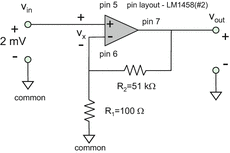
Using the two summing-point constraints, solve the ideal-amplifier circuit shown in the figure if the input voltage has the value of 2 mV.
-
A.
Label and determine the currents in the feedback loop.
-
B.
Determine the output voltage of the amplifier versus the common port.

Problem 5.26
Determine the output voltage of the ideal operational amplifier shown in the figure. The amplifier is driven by a ±10-V dual power supply.

Inverting Amplifier
Problem 5.27
-
A.
Draw the circuit diagram of the basic inverting amplifier configuration.
-
B.
Give the expression for the amplifier gain in terms of the resistances, assuming an ideal operational amplifier.
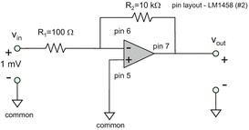
Problem 5.28
Using the two summing-point constraints, solve the ideal-amplifier circuit shown in the figure that follows if the input voltage is 1 mV.
-
A.
Label and determine the currents in the feedback loop.
-
B.
Determine the output voltage of the amplifier versus the common port.

Problem 5.29
Determine the output voltage of the ideal operational amplifier shown in the figure. The amplifier is driven by a ±10-V dual power supply.

Voltage Follower
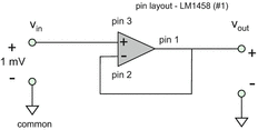
Problem 5.30
-
A.
Using only the first summing-point constraint (SPC), solve the circuit shown in the figure, i.e., determine the output voltage of the amplifier versus the common port.
-
B.
What function does this amplifier have? Why is it important?

Exercises on the Use of the Negative Feedback
Problem 5.31
(A review problem) For three basic ideal-amplifier circuits:
Inverting amplifier |
Non-inverting amplifier |
Voltage follower |
(each includes negative feedback) present
-
1.
A circuit diagram
-
2.
Expression for the amplifier gain
Problem 5.32
Determine the output voltage of amplifier configurations shown in the figure that follows. The amplifier is powered by a ±9-V dual-polarity voltage power supply. Assume an ideal operational amplifier.

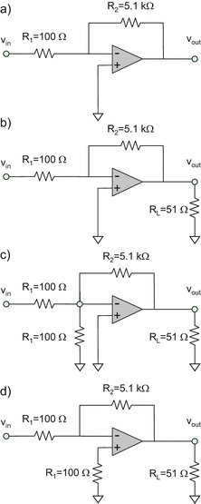
Problem 5.33
Each of the circuits shown in the figures below employs negative feedback. Find the output voltageυ out vs. ground (or common).Hint: The ground symbol in an amplifier circuit usually has thesame meaning as the common port.

Problem 5.34
Each of the circuits shown in the figures below employs negative feedback. Find the output voltage Vout vs. ground (or common).Hint: The ground symbol in the amplifier circuit usually has the same meaning as the common port.

Problem 5.35
Each of the circuits shown in the figures below employs an inverting amplifier.
-
1.
Solve each circuit (findυ out) with an input voltage of 1 mV.
-
2.
Based on this solution, find the closed-loop voltage gainA CL of the corresponding amplifier circuit.

Problem 5.36
An inverting amplifier that achieves high-gain magnitude with a smaller range of resistance values is shown in the figure below. Find its output voltageυ out vs. ground (or common port) and the resulting amplifier gain.

Problem 5.37
The amplifier circuit shown in the figure employs negative feedback.
-
A.
Find the value of the output currenti out if the input current is 1 mA,\( {R}_1=9\kern0.5em \mathrm{k}\Omega, \kern0.5em {R}_2=1\kern0.5em \mathrm{k}\Omega \).
-
B.
Why do you think this amplifier type is known as thecurrent amplifier? To answer this question quantitatively, analytically express the output currenti out (current through the load) in terms of the unknown input currenti out and two arbitrary resistor values,R 1,2.

5.2.4 Mathematics Behind the Second Summing-Point Constraint
Problem 5.38
-
A.
Derive an expression for the closed-loop gain of the non-inverting amplifier based only on the definition of the output voltage\( {\upsilon}_{\mathrm{out}}=A\left({\upsilon}_{\mathrm{in}}^{+}-{\upsilon}_{\mathrm{in}}^{-}\right) \), without using the second summing-point constraint.
-
B.
Determine the exact gain value when
$$ A=2\times {10}^5 $$$$ {R}_1=1\kern0.5em \mathrm{k}\Omega, {R}_2=9\kern0.5em \mathrm{k}\Omega $$

Problem 5.39
-
A.
Derive an expression for the closed-loop gain of the inverting amplifier based only on the definition of the output voltage\( {\upsilon}_{\mathrm{out}}=A\left({\upsilon}_{\mathrm{in}}^{+}-{\upsilon}_{\mathrm{in}}^{-}\right) \), without using the second summing-point constraint.
-
B.
Determine the exact gain value when
5.2.5 Current Flow in the Amplifier Circuit
Problem 5.40
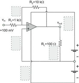
The amplifier circuit shown in the figure below is powered by a ±9-V dual-polarity voltage power supply.
-
A.
Redraw the amplifier schematic in your notes.
-
B.
Show the current direction in every wire of the circuit by an arrow and write the corresponding current value close to each arrow.
Hint: Change the polarity of the input voltage and the voltage sign if you have trouble operating with negative values.

Problem 5.41
Repeat the previous problem for the circuit shown in the figure below.

Problem 5.42
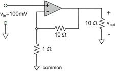
The amplifier shown in the figure below is powered by a ±9-V dual-polarity voltage power supply.
-
A.
Redraw the amplifier schematic in your notes.
-
B.
Show the current direction in every wire of the circuit by an arrow and write the corresponding current value close to each arrow.

Problem 5.43
Repeat the previous problem when the input voltage to the amplifier is −100 mV.
5.2.6 Multiple-Input Amplifier Circuit: Summing Amplifier
Problem 5.44
By solving the amplifier circuit shown in the figure, fill out the table that follows. Assume that\( {R}_0={R}_{\mathrm{F}} \),\( {R}_1={R}_{\mathrm{F}}/2 \), and\( {R}_2={R}_{\mathrm{F}}/4 \).

D 2, V | D 1, V | D 0, V | υ out, V |
0 | 0 | 0 | |
0 | 0 | 5 | |
0 | 5 | 0 | |
0 | 5 | 5 | |
5 | 0 | 0 | |
5 | 0 | 5 | |
5 | 5 | 0 | |
5 | 5 | 5 |
Problem 5.45
The amplifier circuit shown in the figure below employs negative feedback. This configuration is known as a three-bit digital-to-analog converter (DAC) on the base of an R/2R ladder. By solving the amplifier circuit, determine its output voltage in terms of resistancesR, R F, given the input voltages\( {D}_0=0\kern0.5em \mathrm{V},{D}_1=0\kern0.5em \mathrm{V},{D}_2=5\kern0.5em \mathrm{V} \).

Problem 5.46
By solving the amplifier circuit shown in the following figure, determine its output voltage in terms of resistancesR, R F, given the input voltages\( {D}_0=0\kern0.5em \mathrm{V},{D}_1=5\kern0.5em \mathrm{V},{D}_2=0\kern0.5em \mathrm{V} \).

2.3 5.3 Amplifier Circuit Design
5.3.1 Choosing Proper Resistance Values
Problem 5.47
State the limitations on the feedback resistances and the output load resistance of an amplifier circuit.
Problem 5.48
The non-inverting amplifier shown in the figure below has been wired in laboratory.
-
A.
Do you have any concerns with regard to this circuit?
-
B.
If you do, draw the corrected circuit diagram.

5.3.2 Model of a Whole Amplifier Circuit
5.3.3 Input Load Bridging or Matching
Problem 5.49
For three basic amplifier circuits
Inverting amplifier |
Non-inverting amplifier |
Voltage follower |
(each includes negative feedback), present
-
1.
A circuit diagram
-
2.
An expression for the closed-loop amplifier circuit gain
-
3.
An expression for the input resistance (impedance)
-
4.
An expression for output resistance (impedance)
Problem 5.50
-
A.
Explain in your own words the concept of load bridging (impedance bridging).
-
B.
Which amplifier, the non-inverting or inverting, should be subject to load bridging?
Problem 5.51
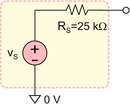
An electromechanical sensor is given by its Thévenin equivalent wherein the sensor voltageυ S is small. The sensor’s equivalent resistanceR S may vary in time; but it is always less than 1 kΩ. An inverting amplifier is needed that generates an amplified version of the sensor’s voltage. The output voltage should be\( \approx -100{\upsilon}_{\mathrm{S}} \). Draw the corresponding circuit diagram and specify one possible set of resistor values.
Problem 5.52
Construct an amplifier circuit matched to a 100-Ω load. The amplifier’s gain is\( \left|{A}_{\mathrm{CL}}\right|=100 \). The sign of the gain (positive or negative) is not important and the input AC signal.
Hint: Multiple solutions many exist. Present at least two solutions.
Problem 5.53
Find the input resistance (impedance) to the amplifier circuit shown in the figure below.

Problem 5.54
Find the input resistance (impedance) to the amplifier circuit shown in the figure below.

5.3.4 Cascading Amplifier Stages
Problem 5.55
For the amplifier circuit shown in the figure, find the output voltage and the input resistance (show units).

Problem 5.56
A sensor with Thévenin voltage (source voltage)\( {\upsilon}_{\mathrm{S}}=2.5\kern0.5em \mathrm{mV} \) shown in the figure is to be connected to an amplifier circuit. An amplified replica of the sensor’s voltage,\( {\upsilon}_{\mathrm{out}}\approx 1000\kern0.15em {\upsilon}_{\mathrm{S}} \), is needed at the circuit’s output.
-
A.
Present one possible circuit diagram and specify all necessary resistor values.
-
B.
Present another (distinct) circuit diagram and specify all necessary resistor values.

Problem 5.57
An amplifier in the configuration shown in the figure below is connected to a sensor with Thévenin (source) voltage\( {\upsilon}_{\mathrm{S}}=25\kern0.5em \mathrm{mV} \). An amplified replica of the sensor’s voltage,\( {\upsilon}_{\mathrm{out}}\approx -100\kern0.15em {\upsilon}_{\mathrm{S}} \), is needed at the output.
-
A.
Do you have any concerns with regard to this circuit?
-
B.
If you do, draw an appropriate circuit diagram.

Problem 5.58
An amplifier circuit is needed with the closed-loop gain\( {A}_{\mathrm{CL}}=+1000 \). The input resistance (impedance) to the circuit should be 5 kΩ. Present two alternative circuit diagrams and specify the necessary resistor values. The first circuit must use inverting amplifiers and the second circuit-non-inverting amplifiers.
Problem 5.59
An amplifier circuit is needed with the closed-loop gain\( {A}_{\mathrm{CL}}=+10,000 \). The input resistance (impedance) to the circuit should be as high as possible. Present the corresponding circuit diagram and specify the necessary resistor values.
Problem 5.60
An amplifier circuit is needed with a positive gain of 1000 ± 20 %. The input resistance (impedance) to the circuit should be 1 kΩ. Present the circuit diagram and specify the necessary resistor values including tolerance.
Problem 5.61
An amplifier circuit is needed with a positive gain of 5000 ± 5 %. The input resistance (impedance) should be as high as possible. Present one possible circuit diagram and specify the necessary resistor values including tolerance.
5.3.5 Amplifier DC Imperfections and Their Cancellation
Problem 5.62
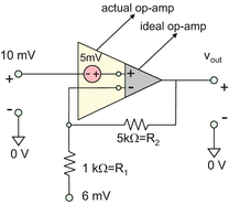
Determine the output voltage to nonideal operational amplifier circuits (with the nonzero input offset voltage) shown in the figures below.

Problem 5.63
Determine the output voltage to nonideal operational amplifier circuits (with nonzero input currents) shown in the figures below. The input terminal is connected directly to the common terminal (grounded). The strength of every bias current source is 100 nA.
Hint: The upper bias current source does not contribute to the solution.

Problem 5.64
For the amplifier circuit shown in the figure below, determine the output voltage. Use\( {R}_1={R}_2=1\kern0.5em \mathrm{k}\Omega \).

Problem 5.65
In the previous problem, denote the terminal voltage of 2 mV byV off, the input voltage of 1 mV byυ in, the output voltage byυ out, and the amplifier gain byA CL. Derive an analytical formula that determinesV off in terms ofV in given that the output voltageυ out to the amplifier is exactly zero.
Problem 5.66
For the amplifier circuit shown in the figure below, determine the output voltage. Use\( {R}_1=1\kern0.5em \mathrm{k}\Omega \) and\( {R}_2=4\kern0.5em \mathrm{k}\Omega \).

Problem 5.67
In the previous problem, denote the terminal voltage of 4 mV byV off, the input voltage of 5 mV byυ in, the output voltage byυ out, and the amplifier gain byA CL. Derive an analytical formula that determinesV off in terms ofυ in given that the output voltage to the amplifier is exactly zero.
Problem 5.68
For the circuit shown in the figure below:
-
A.
Determine the output voltage of the nonideal operational amplifier circuit (with the nonzero input offset voltage).
-
B.
Does the amplifier circuit really follow the ideal-amplifier circuit law:\( {\upsilon}_{\mathrm{out}}={A}_{\mathrm{CL}}{\upsilon}_{\mathrm{in}} \)?
-
C.
What happens if the input voltage changes from 10 mV to 20 mV?

Problem 5.69
Solve the previous problem with the offset voltage in the feedback loop changed from 6 mV to 5 mV.
Problem 5.70
In problem5.68, denote the terminal voltage of 6 mV byV off, the input voltage of 10 mV byυ in, the input offset voltage byV OS, the output voltage byυ out, and the amplifier gain byA CL. Derive an analytical formula that determinesV off in terms ofV OS given that the output voltageυ out to the amplifier must exactly follow the ideal-amplifier gain law:\( {\upsilon}_{\mathrm{out}}={A}_{\mathrm{CL}}{\upsilon}_{\mathrm{in}} \).

Problem 5.71
For two nonideal operational amplifier circuits (with the nonzero input offset voltage) shown in the figures below, determine the necessary offset voltage,V off, which ensures that the output voltage,υ out, to the amplifier exactly follows the ideal-amplifier gain law:\( {\upsilon}_{\mathrm{out}}={A}_{\mathrm{CL}}{\upsilon}_{\mathrm{in}} \). You need to express this voltage in terms of other circuit parameters that are given in figures a) and b).

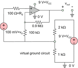
5.3.6 DC-Coupled Single-Supply Amplifier
Problem 5.72
For the single-supply amplifier circuit shown in the figure:
-
A.
Determine the output voltage versus circuit ground (the negative terminal of the voltage power supply).
-
B.
What potential problem do you see with this circuit? How could you fix it?

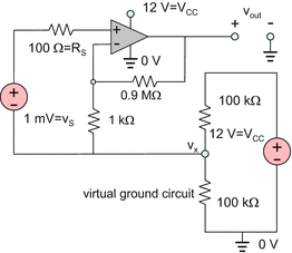
Problem 5.73
For the single-supply amplifier circuit shown in the figure:
-
A.
Determine the output voltage versus circuit ground (the negative terminal of the voltage power supply).
-
B.
Do you see any problem with this circuit?

2.4 5.4 Difference and Instrumentation Amplifiers
5.4.1 Differential Input Signal to an Amplifier
Problem 5.74
The model of an input signal from a three-terminal sensing device is shown in the figure below. What are the differential and common-mode voltages at terminalsa andb?

Problem 5.75
The Wheatstone bridge in Fig. 5.27 is connected to\( \pm {V}_{\mathrm{CC}} \) rails instead of\( +{V}_{\mathrm{CC}} \) and ground. Furthermore,\( {R}_2=1.1{R}_1 \),\( R(x)=1.1{R}_3 \), and\( {V}_{\mathrm{CC}}=6\;\mathrm{V} \). What are the differential and common-mode voltages?
Problem 5.76
The Wheatstone bridge in Fig. 5.27 is connected to ground and\( -{V}_{\mathrm{CC}} \) rails instead of\( +{V}_{\mathrm{CC}} \) and ground. Given that\( {R}_2=1.05{R}_1 \),\( R(x)=1.05{R}_3 \), and\( {V}_{\mathrm{CC}}=6\kern0.5em \mathrm{V} \), determine the differential and common-mode voltages.
5.4.2 Difference Amplifier
Problem 5.77
Design a difference amplifier with a differential gain of 20. Present the circuit diagram and specify one possible set of resistor values. In the circuit diagram, label the input voltages asυ a, υ b and express the output voltage in terms ofυ a, υ b.
Problem 5.78
Repeat the previous problem for a differential gain of 100.
Problem 5.79
Find the output voltage to the difference-amplifier circuits shown in the figures below. Assume the ideal-amplifier model and exact resistance values.

Problem 5.80
Your technician needs to control a process using two sensors with output voltagesυ 1 andυ 2, respectively. The weighted difference in sensor reading,\( \upsilon =1{\upsilon}_1-0.5{\upsilon}_2 \), is critical for the product quality. The technician reads voltageυ 1 and then voltageυ 2 and then uses a calculator to findυ. Help the technician, i.e., sketch for him a difference-amplifier circuit that will directly outputυ to the DMM. The negative terminal of the DMM is always grounded. Specify one possible set of resistor values.
Problem 5.81
Repeat the previous problem when the weighted difference in sensor reading,\( \upsilon =10{\upsilon}_1-5{\upsilon}_2 \), needs to be processed.
Problem 5.82
For the circuit shown in the figure, find the output voltage if the input voltages are\( {\upsilon}_{\mathrm{b}}=1\;\mathrm{V} \) and\( {\upsilon}_{\mathrm{a}}=1.01\;\mathrm{V} \), respectively. Assume the ideal-amplifier model and exact resistance values.

Problem 5.83
-
A.
For the circuits shown in the figures below, find the output voltage if the input voltages are\( {\upsilon}_{\mathrm{a}}=1\;\mathrm{V} \) and\( {\upsilon}_{\mathrm{b}}=1\;\mathrm{V} \), respectively Assumethe ideal amplifier and exact resistance values.
-
B.
What is the value of the common-mode gain in every case?
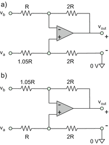

Problem 5.84
For the difference-amplifier circuit shown in the figure below, find thedifferential-mode resistance (impedance) to the amplifier. The differential-mode resistance is defined as the ratio of a voltage of a power supply placed between terminalsa andb to the current that flows through this power supply.

5.4.3 Instrumentation Amplifier
Problem 5.85
-
A.
Why is the original difference amplifier not used as an instrumentation amplifier?
-
B.
Why is the circuit in Fig. 5.31 not used as the instrumentation amplifier?
Problem 5.86
-
A.
Find the differential gain and the common-mode gain for the amplifier circuit shown in Fig. 5.32. The differential output voltage is\( {\upsilon}_{\mathrm{a}}*-{\upsilon}_{\mathrm{b}}* \), and the common-mode output voltage is\( 0.5\left({\upsilon}_{\mathrm{a}}*+{\upsilon}_{\mathrm{b}}*\right) \).
-
B.
Find the differential gain and the common-mode gain for the amplifier circuit shown in Fig. 5.31.
Problem 5.87
Design an instrumentation amplifier with a differential gain of 210. Present the corresponding circuit diagram and specify one possible set of resistance values. In the circuit diagram, label the input voltages asυ a, υ b and express the output voltage in terms ofυ a, υ b.
Problem 5.88
Design an instrumentation amplifier with a differential gain of 1010. Present the corresponding circuit diagram and specify one possible set of resistor values. In the circuit diagram, label the input voltages asυ a, υ b and express the output voltage in terms ofυ a, υ b.
Problem 5.89
The following voltages are measured:\( {\upsilon}_{\mathrm{a}}=3.750\kern0.5em \mathrm{V} \) and\( {\upsilon}_{\mathrm{b}}=3.748\kern0.5em \mathrm{V} \). Find voltages versus circuit ground (common port of the dual supply) for every labeled node in the circuit shown in the figure below. The amplifier circuit is powered by a\( \pm 10-\mathrm{V} \) dual supply. Assume exact resistance values and the ideal-amplifier model.

Problem 5.90
Repeat the previous problem when node 1 is grounded.
Problem 5.91
The following voltages are measured:\( {\upsilon}_{\mathrm{a}}=5.000\;\mathrm{V}\ \mathrm{and}\kern0.5em {\upsilon}_{\mathrm{b}}=5.001\kern0.5em \mathrm{V} \). Find voltages versus circuit ground (common port of the dual supply) for every labeled node in the circuit shown in the figure below. The amplifier circuit is powered by a\( \pm 10-\mathrm{V} \) dual supply. Assume exact resistance values and the ideal-amplifier model.

Problem 5.92
Repeat the previous problem when node 1 is grounded.
Problem 5.93
The following voltages are measured:\( {\upsilon}_{\mathrm{a}}=5.000\kern0.5em \mathrm{V} \) and\( {\upsilon}_{\mathrm{b}}=5.001\kern0.5em \mathrm{V} \). Find voltages versus circuit ground (common port of the dual supply) for every labeled node in the circuit shown in the figure below. The amplifier circuit is powered by a\( \pm 10-\mathrm{V} \) dual supply. Assume exact resistance values and the ideal-amplifier model.

Problem 5.94
-
A.
Find the output voltage for the amplifier circuit shown in the figure below.
-
B.
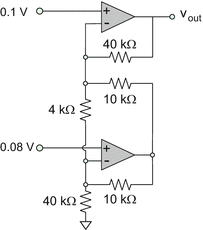
Denote the input voltage of 0.1 V byυ a, the input voltage of 0.08 V byυ b, the 10-kΩ resistor byR 1, the 40-kΩ resistor byR 2, and the 10-kΩ resistor byR G. Express the output voltage in the general form, in terms of two input voltages and the resistances.

2.5 5.5 General Feedback Systems
5.5.1 Signal-flow Diagram of a Feedback System
5.5.2 Closed-Loop Gain and Error Signal
Problem 5.95
The block diagram of Fig. 5.35 is applied to a voltage amplifier.
-
A.
Given the input signal\( {x}_{\mathrm{in}}=10\kern0.5em \mathrm{mV} \), the error signal\( {x}_{\mathrm{e}}=1\kern0.5em \upmu \mathrm{V} \), and the output signal\( {x}_{\mathrm{out}}=1\kern0.5em \mathrm{V} \), determine the open-loop gain and the feedback factor.
-
B.
Given the ratio of input to error signal\( {x}_{\mathrm{in}}/{x}_{\mathrm{e}}=100 \) and the feedback factor of 0.1, determine the open-loop gain.
Problem 5.96
The open-loop gainA in Fig. 5.35 varies between two extreme values of\( A=10,000\pm 2,000 \) (±20 % gain variation) depending on the system parameters. The forward gain block is used in the closed-loop configuration with the feedback factorβ of 0.1. Determine the two extreme values of the closed-loop gain,A CL.
Problem 5.97
The open-loop gainA in Fig. 5.35 is 100,000. The forward gain block is used in the closed-loop configuration with the feedback factorβ of 1. Determine the error signal,x e, if the input voltage signal is 1 mV.
Problem 5.98
The closed-loop gain of a non-inverting amplifier circuit with\( {R}_1=1\kern0.15em \mathrm{k}\Omega, \kern0.15em {R}_2=100\kern0.5em \mathrm{k}\Omega \) is 99. Determine the open-circuit gainA of the amplifier chip.
5.5.3 Application of General Theory to Voltage Amplifiers with Negative Feedback
5.5.4 Voltage, Current, Transresistance, and Transconductance Amplifiers with the Negative Feedback
Problem 5.99
Derive the gain Eq. (5.69) for the amplifier circuits shown in Fig. 5.37.
Problem 5.100
The circuit shown in the figure that follows is a feedback transconductance amplifier. Expressi out in terms ofυ in.

Problem 5.101
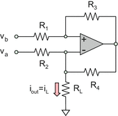
The amplifier circuit shown in the figure that followsis theHowland current source widely used in biomedical instrumentation; its output is the current through the load resistance.
-
A.
Classify the amplifier circuit in terms of four basic amplifier topologies and mention the most important circuit features.
-
B.
Derive its gain equation\( {i}_{\mathrm{out}}=\left({\upsilon}_{\mathrm{a}}-{\upsilon}_{\mathrm{b}}\right)/{R}_2 \) given that\( {R}_1/{R}_3={R}_2/{R}_4 \).

Rights and permissions
Copyright information
© 2016 Springer International Publishing Switzerland
About this chapter
Cite this chapter
N. Makarov, S., Ludwig, R., Bitar, S.J. (2016). Operational Amplifier and Amplifier Models. In: Practical Electrical Engineering. Springer, Cham. https://doi.org/10.1007/978-3-319-21173-2_5
Download citation
DOI: https://doi.org/10.1007/978-3-319-21173-2_5
Publisher Name: Springer, Cham
Print ISBN: 978-3-319-21172-5
Online ISBN: 978-3-319-21173-2
eBook Packages: EngineeringEngineering (R0)