
Abstract
Knowledge of basic circuit analysis
This is a preview of subscription content, log in via an institution.
Buying options
Tax calculation will be finalised at checkout
Purchases are for personal use only
Learn about institutional subscriptionsAuthor information
Authors and Affiliations
Appendices
Summary
Problems
2.1 14.1 Digital Voltage and Binary Numbers
14.1.2 Analog Voltage Versus Digital Voltage
14.1.3 Bit Rate. Clock Frequency. Timing Diagram
Problem 14.1
Describe in your own words the meaning of:
-
1.
Analog voltage
-
2.
Digital voltage
-
3.
A bit
-
4.
A binary number
-
5.
Most significant bit (MSB)
-
6.
Least significant bit (LSB)
Problem 14.2
Convert the following binary numbers:
-
A.
1000001
-
B.
11111
-
C.
111111
-
D.
00001
-
E.
11110000
to decimal numbers.
Problem 14.3
Determine integer (decimal) numbers represented by parallel digital output voltages shown in the following figure.

Problem 14.4
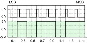
Determine integer (decimal) numbers represented by serial digital output voltages shown in the figure. Sampling is made at the center of each bit interval. In part (c), the least significant bit arrives first at the earliest time moment.

Problem 14.5
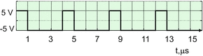
A generic oscilloscope is measuring a periodic voltage clock signal. The oscilloscope window is shown in the following figure.
-
A.
Determine the clock period.
-
B.
Determine the clock frequency (show units).
-
C.
Determine the duty cycle of the clock waveform.
-
D.
Determine Pk-Pk (peak-to-peak) voltage of the clock signal.

Problem 14.6
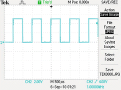
A Tektronix oscilloscope is measuring a voltage clock signal. The oscilloscope window is shown in the following figure.
-
A.
Determine the clock period.
-
B.
Determine the clock frequency (show units).
-
C.
Determine the duty cycle of the clock waveform.
-
D.
Determine Pk-Pk (peak-to-peak) voltage of the clock signal.

Problem 14.7
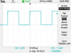
A Tektronix oscilloscope is measuring a voltage clock signal. The oscilloscope window is shown in the following figure.
-
A.
Determine the clock period.
-
B.
Determine the clock frequency (show units).
-
C.
Determine the duty cycle of the clock waveform.
-
D.
Determine Pk-Pk (peak-to-peak) voltage of the clock signal.

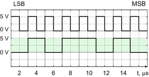
Problem 14.8
The following figure shows a timing diagram: the clock signal and the actual synchronized serial bit stream (the unipolar NRZ code).
-
A.
Determine the clock period.
-
B.
Determine the clock frequency (show units).
-
C.
Determine the bit rate of the bit stream (show units).
-
D.
Decode the corresponding binary number given the LSB/MSB positions (present its decimal equivalent).

Problem 14.9
The following figure shows a timing diagram: the clock signal and the actual synchronized serial bit stream (the polar NRZ code).
-
A.
Determine the clock period.
-
B.
Determine the clock frequency (show units).
-
C.
Determine the bit rate of the bit stream (show units).
-
D.
Decode the corresponding binary number given the LSB/MSB positions (present its decimal equivalent).

14.1.4 Binary Numbers
14.1.5 Hexadecimal Numbers
14.1.6 ASCII Codes and Binary Words
14.1.7 Tri-state Digital Voltage
Problem 14.10
Name two major reasons why the analog computer was surpassed by the digital computer.
Problem 14.11
Describe in your own words the meaning of:
-
1.
A digital word
-
2.
A nibble
-
3.
A byte
Problem 14.12
Without a calculator or MATLAB, convert the following binary numbers to decimal numbers:
-
A.
1010
-
B.
101010
-
C.
11.1
-
D.
10.001
Problem 14.13
Using either a calculator or MATLAB, convert the following binary numbers to decimal numbers:
-
A.
1000001.111111
-
B.
0001111.000010
Problem 14.14
Without a calculator or MATLAB, convert the following decimal numbers to binary numbers:
-
A.
19
-
B.
10
-
C.
1960
-
D.
14.25
Problem 14.15
Using either a calculator or MATLAB, convert decimal numbers that follow to binary numbers. The desired degree of precision is six bits after the binary point:
-
A.
133.33
-
B.
999.125
-
C.
256.256
Problem 14.16
-
A.
How many bits are necessary to represent decimal number 300,000,000 in binary form?
-
B.
How many bytes are necessary?
Problem 14.17
Write down the year of your birth. Without a calculator or MATLAB, convert this decimal number to:
-
A.
Binary number
-
B.
Hexadecimal number
Problem 14.18
Using the ASCII conversion table, write the string USA in terms of:
-
A.
Three decimal numbers
-
B.
Three hexadecimal numbers
-
C.
Three binary numbers
Problem 14.19
Without a calculator or MATLAB, convert hexadecimal numbers that follow to decimal numbers and binary numbers, respectively:
-
1.
1
-
2.
12
-
3.
1A
-
4.
AAA
-
5.
ECE
-
6.
BE
-
7.
CE
Problem 14.20
Using either a calculator or MATLAB, convert hexadecimal numbers that follow to decimal numbers:
-
1.
3F7
-
2.
EE.25
-
3.
555h
-
4.
0x555
Problem 14.21
Convert binary numbers that follow to hexadecimal numbers:
-
1.
01
-
2.
11110101
-
3.
1000000110000000
-
4.
1111111110000001
-
5.
1111111111111111.1111
2.2 14.2 Digital to Analog Converter
14.2.1 Digital to Analog Converter (DAC)
14.2.2 Circuit (A Binary-Weighted-Input DAC)
14.2.3 Underlying Math and Resolution Voltage
Problem 14.22
The DAC circuit from Fig. 14.15 is operating using the virtual-ground condition of the inverting amplifier in order to add up weighted-input currents. With this in mind, a beginning ECE student removes the amplifier from the circuit and puts a common ground reference at the summing node instead. Will the circuit work?
Problem 14.23
-
A.
For an 8-bit binary-weighted-input DAC, express its output voltage through the resolution voltage (LSB voltage), Q, and binary digits d 7, d 6, …, d 0, which corresponds to the input voltages.
-
B.
Find the output voltage when the LSB voltage is 20 mV and \( {d}_7={d}_6\dots ={d}_2=1,{d}_1=0,{d}_0=1 \).
Problem 14.24
A 3-bit binary-weighted digital-to-analog converter (DAC) is shown in the figure. The circuit does not include the inverter. Fill out the table that follows:

D2, V | D1, V | D0, V | υ DAC , V |
0 | 0 | 0 | |
0 | 0 | 5 | |
0 | 5 | 0 | |
0 | 5 | 5 | |
5 | 0 | 0 | |
5 | 0 | 5 | |
5 | 5 | 0 | |
5 | 5 | 5 |
Problem 14.25
Repeat the previous problem for the DAC shown in the following figure.

Problem 14.26
For a 4-bit binary-weighted-input DAC, the input voltages D 3, D 2, D 1, D 0 are either 0 V or 5 V. The resolution voltage Q of 10 mV is required:
-
A.
Present the circuit diagram of a DAC; label the input voltages.
-
B.
Specify one set of possible resistor values.
Problem 14.27
For a 5-bit binary-weighted-input DAC, the input voltages D 4, D 3, D 2, D 1, D 0 are either 0 V or 2.5 V. The resolution voltage Q of 1 mV is required:
-
A.
Present the circuit diagram of a DAC; label the input voltages.
-
B.
Specify one set of possible resistor values.
Problem 14.28
Design a 4-bit binary-weighted-input DAC circuit which attempts to output the analog voltage in the form of a linear time dependence, \( {\upsilon}_{\mathrm{out}}(t)=5\times {10}^5t \left(\mathrm{V}\right) \) over time interval from 0 to 4 μs. The input to the DAC is a binary-counter sequence of all 4-bit binary numbers. The bit width is 0.25 μs; high and low voltages are 5 V and 0 V, respectively:
-
A.
Present the corresponding circuit diagram; specify required DAC resolution voltage (LSB voltage) and necessary resistor values.
-
B.
Plot the input digital voltages to scale versus time.
-
C.
Plot the output voltage to the DAC to scale versus time.
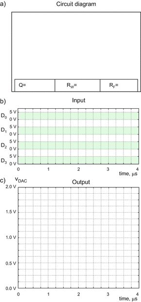

Problem 14.29
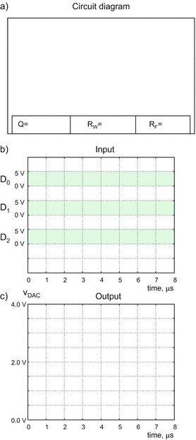
Design a 3-bit binary-weighted-input DAC circuit which attempts to output the analog voltage in the form of a linear time dependence, \( {\upsilon}_{\mathrm{out}}(t)=5\times {10}^5t \left(\mathrm{V}\right) \) over time interval from 0 to 8 μs. The input to the DAC is a binary-counter sequence of all 3-bit binary numbers. The bit width is 1 μs; high and low voltages are 5 V and 0 V, respectively:
-
A.
Present the corresponding circuit diagram; specify the required DAC resolution voltage (LSB voltage) and necessary resistor values.
-
B.
Plot the input digital voltages to scale versus time.
-
C.
Plot the output voltage to the DAC to scale versus time.

Problem 14.30
A 4-bit binary-weighted-input DAC has the resolution voltage, Q, of 0.125 V and the input voltages shown in the following figure. Pin D 3 is accidentally connected to ground. Plot the output voltage of a DAC to scale versus time.

Problem 14.31
Repeat the previous problem for the input voltages shown in the following figure.

14.2.4 DAC Full-scale Output Voltage Range, Resolution, and Accuracy
Problem 14.32
-
A.
For an 8-bit DAC chip, express its output voltage through the full-scale output voltage range, E, and binary digits d 7, d 6, …, d 0, which corresponds to the input voltages.
-
B.
Find the output voltage when the full-scale output voltage range, E, is 6 V and \( {d}_7={d}_6\dots ={d}_2=1,{d}_1=0,{d}_0=1 \).
Problem 14.33
-
A.
For a 10-bit DAC chip, express its output voltage through the full-scale output voltage range, E, and binary digits d 9, d 8, …, d 0, which corresponds to the input voltages.
-
B.
Find the output voltage when the full-scale output voltage range, E, is 10 V and \( {d}_9={d}_8\dots ={d}_3=1,{d}_2={d}_1=0,{d}_0=1 \)
-
C.
Find the resolution voltage of the DAC, Q.
Problem 14.34
A 6-bit DAC and a 8-bit DAC use a 6- and 8-bit binary-counter input sequences in order to produce the analog voltage in the form of a linear time dependence, \( {\upsilon}_{\mathrm{out}}(t)=5\times {10}^5t \left(\mathrm{V}\right) \), over the same time interval from 0 to 10 μs. Determine:
-
1.
DAC resolution in bits (quantization levels)
-
2.
Full-scale output voltage range, E
-
3.
DAC voltage resolution, Q
-
4.
Necessary bit rate, f b
Problem 14.35
An 8-bit DAC and a 10-bit DAC use an 8- and 10-bit binary-counter input sequences in order to produce the analog voltage in the form of a linear time dependence, \( {\upsilon}_{\mathrm{out}}(t)=5\times {10}^6t \left(\mathrm{V}\right) \), over the same time interval from 0 to 1 μs. Determine:
-
1.
DAC resolution in bits (quantization levels)
-
2.
Full-scale output voltage range, E
-
3.
DAC voltage resolution, Q
-
4.
Necessary bit rate, f b
Problem 14.36
For a 3-bit R/2R ladder DAC, the input voltages D 2, D 1, D 0 are either 0 V or 5 V. The resolution voltage Q of 100 mV is required:
-
A.
Present the circuit diagram of a DAC; label the input voltages.
-
B.
Specify one set of possible resistor values.
14.2.5 Other DAC Circuits
Problem 14.37
By solving the amplifier circuit, determine the output voltage of the 3-bit R/2R ladder DAC shown in the following figure given that \( {D}_2=0 \mathrm{V},{D}_1=5 \mathrm{V},{D}_0=0\;\mathrm{V} \).

Problem 14.38
By solving the amplifier circuit, determine the output voltage of the 4-bit R/2R ladder DAC in Fig. 14.18 given that \( {D}_3=0 \mathrm{V},{D}_2=5 \mathrm{V},{D}_1=0 \mathrm{V},{D}_0=0 \mathrm{V} \).

Problem 14.39
An important step in the analysis of the R/2R ladder network is finding Thévenin equivalent for the circuit shown in the figure. Find the Thévenin equivalent and draw the corresponding circuit.

2.3 14.3 Sample-and-Hold Circuit. Nyquist Rate
14.3.1 Analog to Digital Converter (ADC)
14.3.2 A Quick Look at an Analog Sinusoidal Voltage
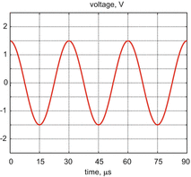
Problem 14.40
-
A.
Determine frequency in Hz, angular frequency in rad/sec, phase, and amplitude of the harmonic voltage signal shown in the following figure.
-
B.
Write the voltage in the form of a cosine function with the corresponding amplitude, frequency, and phase.

Problem 14.41
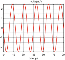
Determine frequency in Hz, angular frequency in rad/s, and amplitude of the harmonic voltage signal shown in the following figure.

Problem 14.42
-
A.
Determine frequency in Hz, angular frequency in rad/s, phase, and amplitude of the harmonic voltage signal shown in the figure.
-
B.
Write the AC voltage in the form of a cosine function, with the corresponding amplitude, frequency, and phase.

14.3.3 Sample-and-Hold Voltage
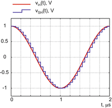
Problem 14.43
For the voltage signal shown in the following figure, determine:
-
A.
Frequency, f, and amplitude, V m, of the analog voltage
-
B.
Sampling interval, T S, and sampling rate, f S, for the sample-and-hold voltage

Problem 14.44*
Plot the figure to the previous problem using MATLAB, introduce a title, and label the axes. Present the text of the corresponding MATLAB script.
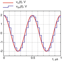
Problem 14.45
For the voltage signal shown in the following figure, determine:
-
A.
Frequency, f, and amplitude, V m, of the analog voltage
-
B.
Sampling interval, T S, and sampling rate, f S, for the sample-and-hold voltage

Problem 14.46*
Plot the figure to the previous problem using MATLAB, introduce a title, and label the axes. Present the text of the corresponding MATLAB script.
14.3.4 Sample-and-Hold Circuit (SH Circuit)
Problem 14.47
Draw the schematic of the sample-and-hold circuit. Explain its operation in steps.
Problem 14.48
The circuit shown in the figure is another modification of the sample-and-hold circuit.
Assuming that the capacitor responds instantaneously:
-
A.
Explain the circuit operation.
-
B.
Sketch its output voltage to scale versus time in the figure the follows.
The switching control voltage is shown on the top of the figure. The switch is closed at high control voltage and is open at low control voltage.

14.3.5 Nyquist Rate
Problem 14.49
An analog voltage is a combination of three sinusoidal harmonics with frequencies 1 MHz, 0.5 MHz, and 0.2 MHz. The voltage amplitudes of the individual sinusoids are 1 V, 1 V, and 5 V. What is the limit on minimum acceptable sampling rate of the sample-and-hold circuit?
Problem 14.50
An analog voltage is a combination of four sinusoidal harmonics with frequencies 0.5 MHz, 0.2 MHz, 1 MHz, and 1.2 MHz. The voltage amplitudes of the individual sinusoids are 5 V, 1 V, 1 V, and 0 V. What is the limit on minimum acceptable sampling rate of the sample-and-hold circuit?
Problem 14.51
Using the figure below, could you demonstrate when the sampling at exactly the Nyquist rate may not be successful?

Problem 14.52
An audio signal (containing all analog sinusoids with frequencies between 20 Hz and 20 kHz) is recorded using a simplified sample-and-hold circuit (the reset switch is omitted) shown in the following figure.

The sample switch closes every:
-
A.
227 μs
-
B.
22.7 μs
-
C.
2.27 μs
then opens momentarily. Which case should be preferred for the minimum memory requirement (for an audio CD)?
2.4 14.4 Analog to Digital Converter
14.4.1 Flash ADC
Problem 14.53
How many comparators would we need for an 8-bit flash ADC? For a 12-bit flash ADC?
Problem 14.54
-
A.
Draw a complete circuit diagram of a 2-bit flash ADC with the full-scale measurement voltage range of 4 V.
-
B.
Fill out the following table:
Range of sample-and-hold voltage υ SH, V | Output of comparator block (3–0) | Output of the priority encoder (binary number d 1 d 0) |
3–4 | ||
2–3 | ||
1–2 | ||
0–1 |
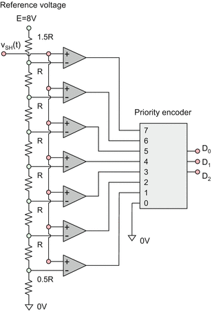
Problem 14.55
-
A.
Draw a complete circuit diagram of a 3-bit flash ADC with the full-scale measurement voltage range of 8 V.
-
B.
Fill out the following table:
Range of sample-and-hold voltage υ SH, V | Output of comparator block (7–0) | Output of the priority encoder (binary number d 3 d 2 d 1 d 0) |
7–8 | ||
6–7 | ||
5–6 | ||
4–5 | ||
3–4 | ||
2–3 | ||
1–2 | ||
0–1 |
14.4.2 ADC Resolution in Bits, Full-scale Input Voltage Range, and Voltage Resolution
Problem 14.56
For a 6-bit ADC determine:
-
A.
Resolution in bits (quantization levels)
-
B.
Voltage resolution, Q
-
C.
Relative accuracy percentage assuming a 1 LSB error
when the full-scale measurement voltage range is 8 V.
Problem 14.57
For an 8-bit ADC determine:
-
A.
Resolution in bits (quantization levels)
-
B.
Voltage resolution, Q
-
C.
Relative accuracy percentage assuming a 1 LSB error
when the full-scale measurement voltage range is 10 V.
14.4.3 ADC Equation and Quantization Error
Problem 14.58
A 5-bit flash ADC follows a mid-rise coding scheme. The reference voltage is 12 V:
-
1.
Present the ADC equation.
-
2.
Determine ADC quantization error.
-
3.
Find ADC output code when the sample-and-hold voltage, υ SH, is 3.1 V.
Problem 14.59
An 8-bit flash ADC follows a mid-tread coding scheme. The reference voltage is 5 V:
-
1.
Present the ADC equation.
-
2.
Determine ADC quantization error.
-
3.
Find ADC output code when the sample-and-hold voltage, υ SH, is 0.2 V.
Problem 14.60
A 3-bit flash ADC is constructed as shown in the following figure:
-
A.
Fill out the table below, which describes the ADC operation. Express all absolute voltage values in terms of the resolution voltage, Q.
-
B.
Based on this table, estimate the quantization error of the ADC in terms of Q.
-
C.
Is this ADC design is better than the mid-rise coding scheme?

Voltage range of υ SH , in terms of Q | Output of comp. block (7–0) | Output of priority encoder (binary number d 2 d 1 d 0) | Voltage decoded back, in terms of Q |
6.5Q–8Q | |||
5.5Q–6.5Q | |||
4.5Q–5.5Q | |||
3.5Q–4.5Q | |||
2.5Q–3.5Q | |||
1.5Q–2.5Q | |||
0.5Q–1.5Q | |||
0–0.5Q |
14.4.4 Successive-Approximation ADC
Problem 14.61
Draw the circuit diagram for a 3-bit successive-approximation ADC.
Problem 14.62
A 4-bit successive-approximation ADC has the input voltage of \( {\upsilon}_{\mathrm{SH}}=1.05 \mathrm{V} \); the DAC resolution voltage is 0.1 V. Determine the sequence of binary states and the final ADC output.
Problem 14.63
A 5-bit successive-approximation ADC has the input voltage of \( {\upsilon}_{\mathrm{SH}}=3.1 \mathrm{V} \); the DAC resolution voltage is 0.2 V. Determine the sequence of binary states and the final ADC output.
Rights and permissions
Copyright information
© 2016 Springer International Publishing Switzerland
About this chapter
Cite this chapter
N. Makarov, S., Ludwig, R., Bitar, S.J. (2016). Analog-to-Digital Conversion. In: Practical Electrical Engineering. Springer, Cham. https://doi.org/10.1007/978-3-319-21173-2_14
Download citation
DOI: https://doi.org/10.1007/978-3-319-21173-2_14
Publisher Name: Springer, Cham
Print ISBN: 978-3-319-21172-5
Online ISBN: 978-3-319-21173-2
eBook Packages: EngineeringEngineering (R0)