
Abstract
Knowledge of complex arithmetic
Access this chapter
Tax calculation will be finalised at checkout
Purchases are for personal use only
Author information
Authors and Affiliations
Appendices
Summary
Problems
2.1 10.1. Theory of the Second-Order RLC Resonator
10.1.1 Self-Oscillating Ideal LC Circuit
10.1.2 Series Resonant Ideal LC Circuit
Problem 10.1
Give an example of a self-oscillating (resonant) mechanical system different from that in Fig. 10.2 of this section.
Problem 10.2
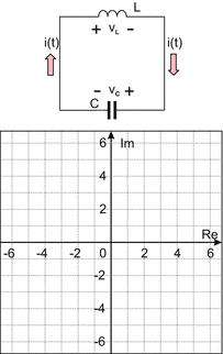
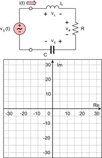
For the self-o scillating circuit shown in the figure below, the circuit current is specified by \( i(t)={I}_{\mathrm{m}} \cos \omega \kern0.1em t \). Given \( {I}_{\mathrm{m}}=200\kern0.5em \mathrm{m}\mathrm{A} \), \( L=0.63\kern0.5em \mathrm{mH},\kern0.5em C=1\kern0.5em \upmu \mathrm{F} \):
-
A.
Determine the undamped resonant frequency f 0.
-
B.
Construct the phasor diagram for phasor voltages V L and V C and phasor current I on the same plot. Assume that every plot division corresponds to 1 V or to 100 mA.

Problem 10.3
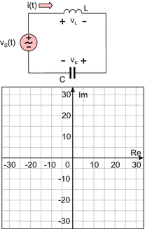
For a series ideal LC circuit shown in the figure below, the voltage source has the form \( {\upsilon}_{\mathrm{S}}(t)={V}_{\mathrm{m}} \cos \omega \kern0.1em t \). Given \( {V}_{\mathrm{m}}=5\kern0.5em \mathrm{V} \), \( L=0.5\kern0.5em \mathrm{mH},\kern0.5em C=1\kern0.5em \upmu \mathrm{F} \):
-
A.
Determine the undamped resonant frequency f 0 of the circuit.
-
B.
Construct the phasor diagram for phasor voltages V S, V L, and V C when the source frequency is 90 % of the resonant frequency.
-
C.
Describe how your phasor diagram would change if the inductance becomes 1 mH instead of 0.5 mH.

Problem 10.4
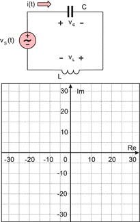
For a series ideal LC circuit shown in the figure below, the voltage source has the form \( {\upsilon}_{\mathrm{S}}(t)={V}_{\mathrm{m}} \cos \omega \kern0.1em t \). Given \( {V}_{\mathrm{m}}=5\kern0.5em \mathrm{V} \), \( L=1\kern0.5em \mathrm{mH},\kern0.5em C=0.5\upmu \mathrm{F} \):
-
A.
Determine the undamped resonant frequency f 0 of the circuit.
-
B.
Construct the phasor diagram for phasor voltages V S, V L, and V C when the source f requency is 111 % of the resonant frequency.
-
C.
Describe how your phasor diagram would change if the capacitance becomes 1 μF instead of 0.5 μF.

10.1.3 Series Resonant RLC Circuit: Resonance Condition
10.1.4 Quality Factor Q of the Series Resonant RLC Circuit
10.1.5 Bandwidth of the Series Resonant RLC Circuit
Problem 10.5
For a generic series resonant RLC circuit with the supply voltage \( {\upsilon}_{\mathrm{S}}(t)={V}_{\mathrm{m}} \cos \omega \kern0.1em t \), resistance R, inductance L, and capacitance C, give the expressions (show units) for:
-
A.
Equivalent circuit impedance at the resonance
-
B.
Resonant frequency
-
C.
Quality factor of the resonant circuit
Problem 10.6
Describe the physical meaning of the quality factor of the series RLC resonator circuit in your own words.
Problem 10.7
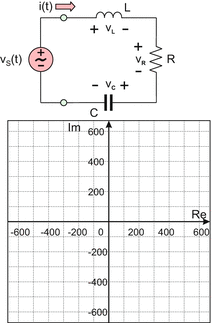
In the series resonant RLC circuit shown in the figure that follows, given \( {V}_{\mathrm{m}}=1\kern0.3em \mathrm{V},\kern0.3em L=1\kern0.3em \mathrm{mH},C=80\kern0.3em \mathrm{pF},\kern0.35em R=10\kern0.3em \Omega \):
-
A.
Determine resonant frequency and the Q-factor.
-
B.
Determine resonant phasor current and phasor voltages V R, V L, and V C; construct the phasor diagram. Assume voltage scale in volts and current scale in milliamperes.
-
C.
Determine the real-valued circuit current i(t) and the inductor/capacitor voltages υ L(t), υ C(t) at resonance.

Problem 10.8
In the series resonant RLC circuit shown in the figure below, given \( {V}_m=5\ \mathrm{V},\kern0.5em L=30\kern0.5em \upmu \mathrm{H},\ C=0.48\kern0.5em \mathrm{nF},\kern0.5em R=50\kern0.5em \Omega \):
-
A.
Determine resonant frequency and the Q-factor.
-
B.
Determine resonant phasor voltages V R, V L, and V C; construct the phasor diagram.
-
C.
Determine the real-valued resistor voltage υ R(t) and the inductor/capacitor voltages υ L(t), υ C(t) at the resonance.

Problem 10.9
A series resonant LC circuit is driven by a laboratory AC voltage source with an amplitude \( {V}_{\mathrm{m}}=12\kern0.5em \mathrm{V} \) and an internal resistance of 50 Ω (a function generator). Which value should the ratio L/C have to obtain the amplitude of the capacitor voltage equal to 200 V at the resonance?
Problem 10.10
A series resonant RLC circuit is needed with the resonant frequency of 1 MHz and a Q-factor of 100. The circuit resistance is 10 Ω. Determine the necessary values of L and C.
Problem 10.11
Describe the physical meaning of the resonance bandwidth of the series resonant RLC circuit in your own words.
Problem 10.12
A series resonant RLC circuit has the resonant frequency of 1 MHz and the quality factor of 10. Create the Bode plot for the amplitude of the circuit current normalized by its maximum value at the resonance over frequency band from 0.5 to 2 MHz.

Problem 10.13
Determine the bandwidth, B, of the series resonant RLC circuit with the resonant frequency of 1 MHz and a Q-factor of 100.
Problem 10.14
A series resonant RLC circuit is needed with the resonant frequency of 1 MHz and the bandwidth of 10 kHz. Given the circuit resistance of 10 Ω, determine L and C.
Problem 10.15
For the RLC circuit block shown in the figure, establish the resonant frequency in terms of component values.
Hint: The resonance is defined by the condition of the purely real equivalent impedance between terminals a and b. In other words, \( \mathrm{I}\mathrm{m}\left({\mathbf{Z}}_{\mathrm{eq}}\right)=0 \) at the resonance.

Problem 10.16
Repeat the previous problem for the circuit shown in the figure that follows.

10.1.6 Parallel Resonant RLC Circuit: Duality
Problem 10.17
For a generic parallel RLC resonant circuit with the supply current \( {i}_{\mathrm{S}}(t)={I}_{\mathrm{m}} \cos \omega t \), resistance R, inductance L, and capacitance C, give the expressions (show units) for:
-
A.
Equivalent circuit impedance at the resonance
-
B.
Resonant frequency
-
C.
Quality factor of the resonant circuit
Problem 10.18
In the parallel resonant RLC circuit shown in the figure that follows, given \( {I}_{\mathrm{m}}=0.5\kern0.3em \mathrm{A},\kern0.5em L=30\kern0.3em \upmu \mathrm{H},C=0.43\kern0.3em \upmu \mathrm{F},\kern0.5em R=50\kern0.3em \Omega \):
-
A.
Determine the resonant frequency and the Q-factor.
-
B.
Determine resonant phasor currents I R, I L, and I C; construct the phasor diagram.
-
C.
Determine the real-valued resistor current i R(t) and the inductor/capacitor currents i L(t), i C(t) at the resonance.

Problem 10.19
Determine the bandwidth, B, of the parallel resonant RLC circuit with the resonant frequency of 0.5 MHz and a Q-factor of 50.
Problem 10.20
A parallel resonant RLC circuit is needed with the resonant frequency of 1 MHz and the bandwidth of 10 kHz. Given the circuit resistance of 100 Ω, determine L and C.
2.2 10.2: Construction of Second-Order RLC Filters
10.2.1 Second-Order Band-Pass RLC Filter
10.2.2 Second-Order Low-Pass RLC Filter
10.2.3 Second-Order High-Pass RLC Filter
10.2.4 Second- Order Band-Reject RLC Filter
Problem 10.21
-
A.
Draw the circuit diagram of the second-order RLC band-pass filter. Label R, L, and C.
-
B.
Show the input and output ports (input and output voltages)
-
C.
Define the resonant frequency and the Q-factor of the filter circuit.
Problem 10.22
A band -pass RLC filter is required with the center (resonant) frequency of 100 kHz and the half-power bandwidth, B, of 20 kHz.
-
A.
Create its amplitude Bode plot in the frequency band from 10 kHz to 1 MHz.
-
B.
Label the filter passband.
-
C.
Determine the necessary values of L and C given \( R=20\kern0.5em \Omega \).

Problem 10.23
-
A.
Draw the circuit diagram of the second-order RLC low-pass filter. Label R, L, and C.
-
B.
Show the input and output ports (input and output voltages)
-
C.
Define the resonant frequency and the Q-factor of the filter circuit.
-
D.
Which Q-factor is required for the maximally flat response?
-
E.
What is the filter’s half-power frequency for the maximally flat response?
Problem 10.24
A low-pass RLC filter is required with the passband from 0 to 1 MHz. Create amplitude Bode plots for the filter in the frequency band from 100 kHz to 10 MHz given the resonant frequency of the filter circuit of 1 MHz and
-
A.
\( Q=5 \)
-
B.
\( Q=1/\sqrt{2} \)
-
C.
\( Q=0.2 \)

Problem 10.25*
Generate Fig. 10.4 of this section, the Bode plots for the low-pass filter using MATLAB.
Problem 10.26
-
A.
Draw the circuit diagram of the second-order RLC high-pass filter. Label R, L, and C.
-
B.
Show the input and output ports (input and output voltages)
-
C.
Define the resonant frequency and the Q-factor of the filter circuit.
-
D.
Which Q-factor is required for the maximally flat response?
-
E.
What is the filter’s half-power frequency for the maximally flat response?
Problem 10.27
A high-pass RLC filter is required with the passband from 0 to 1 MHz. Create amplitude Bode plots for the filter in the frequency band from 100 kHz to 10 MHz given the resonant frequency of the filter circuit of 1 MHz and
-
A.
\( Q=10 \)
-
B.
\( Q=1/\sqrt{2} \)
-
C.
\( Q=0.1 \)
Problem 10.28
-
A.
Draw the circuit diagram of the second-order RLC band-reject filter. Label R, L, and C.
-
B.
Show the input and output ports (input and output voltages)
-
C.
Define the resonant frequency and the Q-factor of the filter circuit.
Problem 10.29
A band-reject RLC filter is required with the center (resonant) frequency of 100 kHz and the half-power bandwidth, B, of 20 kHz.
-
A.
Create its amplitude Bode plot in the frequency band from 10 kHz to 1 MHz.
-
B.
Label the filter passband.
-
C.
Determine the necessary values of L and C given \( R=20\kern0.5em \Omega \).

10.2.6. Second-Order RLC Filters Derived from the Parallel RLC Circuit
Problem 10.30
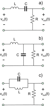
Second-order RLC filters may be constructed either on the basis of the series RLC circuit or on the basis of the parallel RLC circuit. The undamped resonant frequency, \( {f}_0=1/\left(2\pi \sqrt{LC}\right) \), which is present in the filter equations, remains the same in either case. However, the quality factor does not. Three unknown second-order RLC filter circuits are shown in the figure that follows.
-
A.
Determine the filter function (band-pass, low-pass, high-pass, or band-reject).
-
B.
By analyzing filter’s natural structure (after shorting out the input voltage source), determine the expression for the filter quality factor.

2.3 10.3. RLC Circuits for Near-Field Communications and Proximity Sensors
10.3.1 Near-Field Wireless Link
10.3.2 Transmitter Circuit
10.3.3 Receiver Circuit
10.3.4 Application Example: Near-Field Wireless Link in Laboratory
10.3.5 Application Example: Proximity Sensors
Problem 10.31
Describe the concept and purpose of the near-field wireless link in your own words. Think of an example where the link may be used solely for the power transfer.
Problem 10.32
In the circuit shown in the following figure, a capacitor C is introduced in series with an ideal coil having inductance L in order to set up a series resonant RLC circuit and increase the amplitude of the magnetic flux density \( \overrightarrow{B} \) oscillating at 1 MHz. Determine the ratio of the magnetic flux amplitudes
with and without the capacitor anywhere in space given that \( L=100\kern0.5em \upmu \mathrm{H},\ R=25\kern0.5em \Omega \).

Problem 10.33
Given the operation frequency (center band frequency) of \( {f}_0=1\kern0.5em \mathrm{MHz} \) and \( {V}_{\mathrm{m}}=1\kern0.5em \mathrm{V},\kern0.5em L=100\kern0.5em \upmu \mathrm{H},R=20\kern0.5em \Omega \), plot to scale the amplitude of the circuit current as a function of source frequency for the original (RL) and modified (resonant RLC) circuits in the figure to the previous problem over the frequency band from 0.5 to 1.5 MHz. Label the amplitude values at the operation frequency.
Problem 10.34
In the circuit shown in the figure that follows, a receiver coil antenna is subject to an external magnetic field oscillating at 1 MHz. A capacitor C is introduced in parallel with the coil having inductance L and series resistance R in order to set up a series resonant RLC circuit and increase the amplitude of the output voltage υ out(t). Determine the ratio of the output voltage amplitudes with and without the capacitor given that \( L=1000\kern0.5em \upmu \mathrm{H},\ R=10\kern0.5em \Omega \).

Problem 10.35
Given the operation frequency (center band frequency) of \( {f}_0=1\kern0.5em \mathrm{MHz} \) and \( {\upsilon}_{\mathrm{emf}}(t)={V}_{\mathrm{m}} \cos \left(\omega t\right) \), \( {V}_{\mathrm{m}}=1\kern0.5em \mathrm{mV},\kern0.5em L=500\kern0.5em \upmu \mathrm{H},\ R=50\kern0.5em \Omega \), plot to scale the amplitude of the output voltage as a function of source frequency for the original (RL) and modified (resonant series RLC) circuits in the figure to the previous problem over the frequency band from 0.5 to 1.5 MHz. Label the amplitude values at the operation frequency.
Problem 10.36
In the circuit shown in the figure below, a receive coil antenna is subject to an external magnetic field oscillating at 1 MHz. A capacitor C is introduced in parallel with the coil having inductance L and series resistance R in order to set up a series resonant RLC circuit and increase the amplitude of the output voltage υ out(t). Determine the output voltage amplitudes with and without the capacitor given that \( {\upsilon}_{\mathrm{emf}}(t)=1 \cos \left(\omega \kern0.1em t\right)\kern0.5em \left[\mathrm{mV}\right] \) and that \( L=1000\kern0.5em \upmu \mathrm{H},\ R=10\kern0.5em \Omega, {R}_f=100\kern0.5em \Omega \).

Rights and permissions
Copyright information
© 2016 Springer International Publishing Switzerland
About this chapter
Cite this chapter
N. Makarov, S., Ludwig, R., Bitar, S.J. (2016). Second-Order RLC Circuits. In: Practical Electrical Engineering. Springer, Cham. https://doi.org/10.1007/978-3-319-21173-2_10
Download citation
DOI: https://doi.org/10.1007/978-3-319-21173-2_10
Publisher Name: Springer, Cham
Print ISBN: 978-3-319-21172-5
Online ISBN: 978-3-319-21173-2
eBook Packages: EngineeringEngineering (R0)