
Abstract
In this chapter, several transistor circuit configurations are considered. These circuits generally involve more than one transistor and can be implemented in a wide range of applications as well as perform some special functions. In this chapter, the design and application of many of these circuits will be discussed. After completing the chapter, the reader will be able to:
Access this chapter
Tax calculation will be finalised at checkout
Purchases are for personal use only
Bibliography
R.L. Boylestad, L. Nashelsky, Electronic Devices and Circuit Theory, 11th edn. (Pearson Education, New Jersey, 2013)
Vishay Siliconix, FETS as Voltage-Controlled Resistors (1997, March)
Author information
Authors and Affiliations
Problems
Problems
-
1.
Draw the equivalent circuit of the two-stage amplifier in Fig. 5.81. Determine the voltage gain Vo/Vs and hence the current gain Io/Is. Assume hfe = 100 for both transistors.
Fig. 5.81 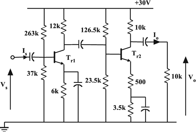
Circuit for Question 1
-
2.
Draw the equivalent circuit of the two-stage amplifier in Fig. 5.82. Determine the voltage gain Vo/Vs and hence the current gain Io/Is. Assume hfe = 200 for both transistors.
Fig. 5.82 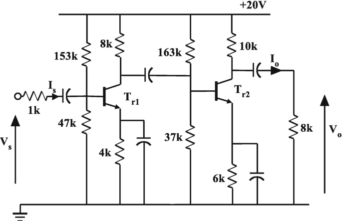
Circuit for Question 2
-
3.
Draw the equivalent circuit of the two-stage amplifier in Fig. 5.83. Determine the voltage gain Vo/Vs and hence the current gain Io/Is. Assume hfe = 100 for both transistors.
Fig. 5.83 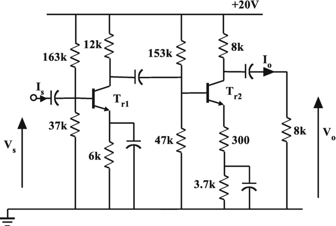
Circuit for Question 3
-
4.
Draw the equivalent circuit of the two-stage amplifier in Fig. 5.84. Determine the voltage gain Vo/Vs and hence the current gain Io/Is. Assume hfe = 100 for both transistors.
Fig. 5.84 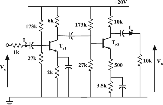
Circuit for Question 4
-
5.
Using the two-stage design in Fig. 5.7 and a 40-volt supply, design a two-stage amplifier that can drive a low-impedance load. Determine the voltage gain of the amplifier. Determine the value of the resistor that can be introduced in the emitter of the first stage as shown in Fig. 5.8 in order to lower the voltage gain to −25.
-
6.
Design a two-stage amplifier having a JFET input stage using the topology of Fig. 5.9 and a 25-volt supply. Use a JFET with VP = − 5 volts and IDSS = 5 mA. Determine the voltage gain of the circuit, and state the main advantage of the JFET stage.
-
7.
Design a low input impedance two-stage amplifier using the circuit of Fig. 5.10 and a 20-volt supply. Determine the input and output impedances as well as the voltage gain.
-
8.
Using the configuration in Fig. 5.85, design a direct coupled amplifier with high gain. Use a supply voltage of 26 V, and calculate the gain of your circuit.
Fig. 5.85 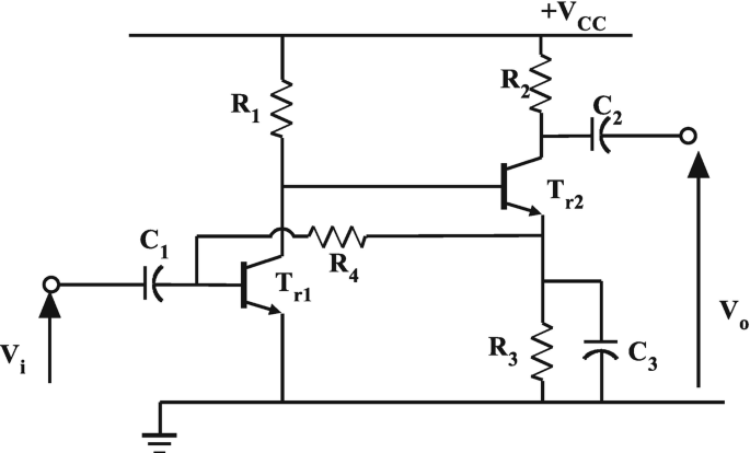
Circuit for Question 8
-
9.
Explain the principle of bootstrapping, and use the technique to increase the gain of the circuit in Question 8.
-
10.
Replace the transistor in the first stage of Fig. 5.85 by a JFET, and re-design the circuit.
-
11.
Design a common emitter amplifier using a pnp Darlington package having βD = 2000 and a 30-volt supply. Calculate the voltage gain of your circuit.
-
12.
Introduce partial bypassing of the emitter resistor in Question 11 in order to achieve a gain of 50.
-
13.
Show that the current gain of a Darlington pair is approximately equal to the product of the current gains of the two transistors making up the pair.
-
14.
Design a common collector amplifier using a Darlington package having βD = 1000 and a 32-volt supply. Calculate the input impedance of your circuit.
-
15.
Apply bootstrapping in order to increase the input impedance of the circuit and estimate the value of this impedance.
-
16.
Show that current gain of a feedback pair is approximately equal to the product of the current gains of the two transistors making up the pair.
-
17.
Derive the voltage gain of a feedback pair in a common emitter configuration, and show that it is significantly higher than either the Darlington pair or a single BJT.
-
18.
Design a circuit using BJTs in a feedback pair to have a gain of 8. Use a supply voltage of 15 volts.
-
19.
Repeat the design in Question 18 with a JFET as the input transistor.
-
20.
Using the configuration in Fig. 5.86, design a constant current source that produces a current of I = 5 mA from a 15-volt supply.
Fig. 5.86 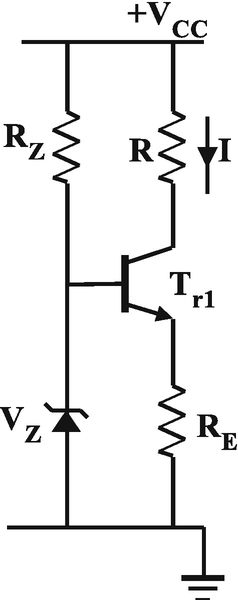
Circuit for Question 20
-
21.
Using the basic circuit of Question 20, show how a pnp transistor can be used to supply a constant current to a grounded load.
-
22.
Using the configuration in Fig. 5.87, design a constant current source that produces a current of 0.5 mA from a 15-volt supply.
-
23.
Repeat the design in Question 22 using pnp transistors.
-
24.
Using a JFET having VP = − 4 volts and IDSS = 4 mA, design a constant current source with current value 1 mA. Determine the current if RS = 0.
-
25.
Design a two-transistor current mirror giving a constant current of 0.5 mA using a 12-volt supply.
-
26.
Design a Wilson current mirror to deliver a constant current of 1.5 mA using a 16-volt supply.


Circuit for Question 22
-
27.
In Fig. 5.88 determine I1, I2, V1 and V2.
-
28.
In Fig. 5.89 determine I1, I2, I3 and I4.
-
29.
In Fig. 5.90 determine I1, I2, V3 and V4.
-
30.
In Fig. 5.91 determine I1, I2, I3 and I4.
-
31.
Using the circuit of Fig. 5.92, design a cascode amplifier to operate from a 32-volt supply, and determine the voltage gain of the circuit.
-
32.
Using a bipolar 15-volt supply, set up a two-transistor differential amplifier with each transistor having 1 mA quiescent current. Use matched transistors, equal collector resistors and design for maximum symmetrical swing.
-
33.
A bipolar junction transistor is being used to switch 12 volts across a 10 k load. Using an npn transistor with β = 150, design a simple switching circuit that is fully on when driven by a 5-volt input.
-
34.
Using an enhancement MOSFET design a switch to drive a 12-volt 5 mA relay from a 12-volt supply. The device has a threshold voltage of 3 volts.
-
35.
Investigate the properties and characteristics of a negative temperature coefficient thermistor. Using such a thermistor and the circuit shown in Fig. 5.93, design a heat sensing system that sounds an alert when the ambient temperature reaches a particular value.

Circuit for Question 27

Circuit for Question 28

Circuit for Question 29

Circuit for Question 30

Circuit for Question 31

Circuit for Question 35
Rights and permissions
Copyright information
© 2021 Springer Nature Switzerland AG
About this chapter

Cite this chapter
Gift, S.J.G., Maundy, B. (2021). Multiple Transistor and Special Circuits. In: Electronic Circuit Design and Application. Springer, Cham. https://doi.org/10.1007/978-3-030-46989-4_5
Download citation
DOI: https://doi.org/10.1007/978-3-030-46989-4_5
Published:
Publisher Name: Springer, Cham
Print ISBN: 978-3-030-46988-7
Online ISBN: 978-3-030-46989-4
eBook Packages: EngineeringEngineering (R0)