
Abstract
This chapter focuses mainly on the drain-extended MOS (DEMOS) transistor and on the lateral double-diffused MOS (LDMOS) transistor for high-voltage/high-power applications. In both cases, the drain is extended with a lightly doped region, referred to as the drift region, to sustain the high voltage. The chapter begins with an analysis of the drift region and its optimization, typically by reduced surface field (RESURF) techniques. The transistor switching performance is then analyzed, followed by a discussion of DEMOS and LDMOS design considerations and characteristics. High-voltage and high-current effects are then described, including quasi-saturation (QS), body current, on-state breakdown, and safe operating area (SOA). The chapter concludes with selected high-voltage device applications.
Access this chapter
Tax calculation will be finalised at checkout
Purchases are for personal use only
Notes
- 1.
Epitaxy is the process of growing a single-crystal film on a single-crystal substrate.
References
D. Riccardi, A. Causio, I. Filippi, A. Paleari, L.V.A. Pregnolato, P. Galbiati, BCD8 from 7 V to 70 V: a new 0.18 μm technology platform to address the evolution of applications towards smart power ICs with high logic contents. IEEE Proc. ISPSD, (2007), pp. 73–76
S. Pendharkar, R. Pan, T. Tamura, B. Todd, T. Efland, 7 to 30 V state-of-art power device implementation in 0.25 μm LBC7 BiCMOS-DMOS process technology.. IEEE Proc. ISPSD, (2004), pp. 419–422
H. Yang, W.-G. Min, X. Lin, V. Newenhouse, J. Huber, H. Xu, Z. Zhang, B. Peterson, J.K. Zuo, Low-leakage SMARTMOS 10 W technology at 0.13 μm node with optimized analog, power, and logic devices for SOC design. VLSI-TSA, (2008), pp. 111–114
H.L. Chou, P.C. Su, J.C.W. Ng, P.L. Wang, H.T. Lu, C.J. Lee, W.J. Syue, S.Y. Yang, Y.C. Tseng, C.C. Cheng, C.W. Yao, R.S. Liou, Y.C. Jong, J.L. Tsai, J. Cai, H.C. Tuan, C.F. Huang, J. Gong, 0.18 μm BCD technology platform with best-in-class 6 V to 70 V power MOSFETs. IEEE Proc. ISPSD, (2012), pp. 401–404
I-Y. Park et al., BD180 – a new 0.18 μm BCD (Bipolar-CMOS-DMOS) technology from 7 V to 60 V. IEEE Proc. ISPSD, (2008), pp. 64–67
H.J. Sigg, G. Vendelin, T.P. Cauge, J. Kocsis, D-MOS transistor for microwave applications. IEEE Trans. Electron Dev. 19(1), 45–53 (1972)
C. Anghel, N. Hefyene, A. M. Ionescu, M. Vermandel, B. Bakeroot, J. Doutreloigne, R. Gillon, S. Frere, C. Maier, Y. Mourier, Investigations and physical modelling of saturation effects in Lateral DMOS transistor architectures based on the concept of intrinsic drain voltage. ESSDERC, (2001), pp. 399–402
J.A. Appels, H.M.J. Vaes, High voltage thin layer devices (RESURF devices). IEEE IEDM Tech. Digest, (1979), pp. 238–241
C. Hu, Optimum doping profile for minimum ohmic resistance and high-breakdown voltage. IEEE Trans. Electron Dev. ED-26(3), 343–344 (1979)
J. Baliga, Fundamentals of Power Semiconductor Devices (Springer, New York, 2008)
A. Ludikhuize, A review of RESURF technology. IEEE Proc. ISPSD, (2000), pp. 11–18
C.Y. Tsai, J. Arch, T. Efland, J. Erdeljac, L. Hutter, J. Mitros, J.Y. Yang, and H.T. Yuan, Optimized 25 V, 0.34 mΩcm2 very-thin-RESURF (VTR), drain-extended IGFETs in a compressed BiCMOS process. IEEE IEDM Tech. Digest, (1996), pp. 469–472
M. Imam, Z. Hossain, M. Quddus, J. Adams, C. Hoggatt, T. Ishiguro, R. Nair, Design and optimization of double-RESURF high-voltage lateral devices for a manufacturable process. IEEE Trans. Electron Dev. 50(7), 1697–1701 (2003)
Z. Hossain, M. Imam, J. Fulton, M. Tanaka, Double-RESURF 700 V N-channel LDMOS with best-in-class on-resistance. IEEE Proc. ISPSD, (2002), pp. 137–140
D.R. Disney, A.K. Paul, M. Darwish, R. Basecki, V. Rumennik, A new 800 V lateral MOSFET with dual conduction paths. IEEE Proc. ISPSD, (2001), pp. 399–402
Y. Shan, Q. Ming, Y. Zhang, B. Zhang, Design of 700 V triple RESURF nLDMOS with low on-resistance. J. Semiconductors 32(11), 114002-1–114002-4 (2011)
Z. Hossain, Determination of manufacturing RESURF process window for a robust 700 V double resurf LDMOS transistor. IEEE Proc. ISPSD, (2008), 133–136
Z. Hossain, T. Ishigwo, L. Tu, H. Corleto, F. Kuramae, R. Nair, Field-plate effects on the breakdown voltage of an integrated high-voltage LDMOS transistor. IEEE Proc. ISPSD, (2004), pp. 237–240
E. Flack, W. Gerlach, J. Korec, Influence of interconnections onto the breakdown voltage of planar high-voltage p-n junction. IEEE Trans. Electron Dev. 40(2), 439–447 (1993)
N.C. Moon, K.W. Kwon, C.J. Lee, K.S. Sung, B.S. Kim, K.D. Yoo, H.S. Park, Design and optimization of 700 V HVIC technology with multi-ring isolation structure. IEEE Proc. ISPSD, (2013), pp. 151–154
V.A.K. Temple, Junction termination extension (JTE), a new technique for increasing avalanche breakdown voltage and controlling surface electric fields in p-n junctions. IEEE IEDM Tech. Digest, (1977), pp. 423–426
V.A.K Temple and W. Tantraporn, “Junction termination for near-ideal breakdown voltage in p-n junctions,” IEEE Trans. Electron Dev., ED-33(10), 1601–1608, 1986
J.K. Oh, M.W. Ha, M.K. Han, Y.I. Choi, A new junction termination method employing shallow trench filled oxide. IEEE Electron Dev. Lett. 25(1), 16–18 (2004)
L. Théolier, H. Mahfoz-Kotb, K. Isoird, F. Morancho, A new junction termination using a deep trench filled with BenzoCycloButene. IEEE Electron Dev. Lett. 30(6), 667–669 (2009)
V. Krishnamurthy, A. Gyure, P. Francis, Simple gate charge (Qg) measurement technique for on-wafer statistical monitoring and modeling of power semiconductor devices. IEEE ICMTS, (2011), pp. 98–100
P. Chimento, G. Lazzaro, S. Musumeci, A. Raciti, Analysis and comparison of low-voltage MOSFET devices with planar and trench-gate layouts. Conf. Integrated Power Systems (CIPS), (2006), pp. 1–6
N. Yasuhara, K. Matsushita, K. Nakayama, B. Tanaka, S. Hodama, A. Nakagawa, K. Nakamura, Low gate charge 30 V N-channel LDMOS for DC-DC converters. IEEE Proc. ISPSD, (2003), pp. 186–189
S. Xu, J. Korec, D. Jauregui, C. Kocon, S. Molly, H. Lin, G. Daum, S. Perelli, K. Barry, C. Pearce, O. Lopez, J. Herbsommer, NexFET A new power device. IEEE IEDM, (2009), pp. 145–148
Y.K. Choi, I.Y. Park, H.C. Lim, M.Y. Kim, C.J. Yoon, N.J. Kim, K.D. Yoo, L.N. Hutter, A versatile 30 V analog CMOS process in a 0.18 μm technology for power management applications. IEEE Proc. ISPSD, (2011), pp. 219–222
A. Mai, H. Rucker, Drain-extended MOS transistors capable for operation at 10 V and at radio frequencies. ESSDERC, (2010), pp. 110–113
J. Sonsky, A. Heringa, Dielectric Resurf: Breakdown voltage control by STI layout in standard CMOS. IEEE IEDM Tech. Digest, (2005), pp. 385–388
A. Heringa, J. Sonsky, J.J. Perez-Gonzalez, R.Y. Su, P.Y. Chiang, Innovative lateral field plates by gate fingers on STI regions in deep submicron CMOS. IEEE Proc. ISPSD, (2008), pp. 271–274
K.Y. Ko, I.Y. Park, Y.K. Choi, C.J. Yoon, J.H. Moon; K.M. Park; H.C. Lim, S.Y. Park, N.J. Kim, K.D. Yoo, L.N. Hutter, BD180LV – 0.18 μm BCD technology with best-in-class LDMOS from 7 V to 30 V. IEEE Proc. ISPSD, (2010), pp. 71–74
R. Pan, B. Todd, P. Hao, R. Higgins, D. Robinson, V. Drobny, W. Tian, J.L. Wang, J. Mitros, M. Huber, S. Pillai, S. Pendharkar, High voltage (up to 20 V) devices implementation in 0.13 μm BiCMOS process technology for system-on-chip (SOC) design. IEEE Proc. ISPSD, (2006), pp. 1–4
J. Lutz et al., Power Semiconductor Devices (Springer, Berlin, Heidelberg, 2011)
J. Smith, A. Tessmer, L. Springer, P. Madhani, J. Erdeljac, J. Mitros, T. Efland, C.Y. Tsai, S. Pendharkar, L. Hutter, A 0.7 μm linear BiCMOS/DMOS technology for mixed-signal/power applications. IEEE BCTM, (1997), pp. 155–157
H. Chang, J.J. Jang, M.H. Kim, E.K. Lee, D.E. Jang, J.S. Park, JH. Jung, C.J. Yoon, S.R. Bae, C.H. Park, Advanced 0.13 μm smart power technology from 7 V to 70 V. IEEE Proc. ISPSD, (2012), pp. 217–220
K. Shirai, K. Yonemura, K. Watanabe, K. Kimura, Ultra-low on-resistance LDMOS implementation in 0.13 μm CD and BiCD process technologies for analog power ICs. IEEE Proc. ISPSD, (2009), pp. 77–79
T. Efland, C.T. Tsai, S. Pendharkar, Lateral thinking about power devices (LDMOS),” IEEE IEDM Tech. Digest, (1998), pp. 679–682
M.L. Kniffin, R. Thoma, J. Victory, Physical compact modeling of layout dependent metal resistance in integrated LDMOS power devices. ISPSD, (2000), pp. 173–176
M. Darwish, J. Huang, M. Liu, M.S. Shekar, R. Williams, M. Cornel, Scaling issues in lateral power MOSFETs. ISPSD, (2001), pp. 329–332
T. Efland; D. Abbott; V. Arellano; M. Buschbom; W. Chang; C. Hoffart; L. Hutter; Q. Mai; I. Nishimura; S. Pendharkar; M. Pierce; C.C. Shen, C.M. Thee, H. Vanhorn, C. Williams, LeadFrameOnChip offers integrated power bus and bond over active circuit. ISPSD, (2001), pp. 65–68
C. Contiero, P. Galbiati, M. Palmieri, I. Vecchi, LDMOS implementation by large tilt implant in 0.6 μm BCD5 process, flash memory compatible. IEEE Proc. ISPSD, (1996), pp. 75–78
A. Moscatelli, A. Merlini, G. Croce, P. Galbiati, C. Contiero, LDMOS implementation in a 0.35 μm BCD technology (BCD6). IEEE Proc. ISPSD, (2000), pp. 323–326
T.N. Buti, S. Ogura, N. Rovedo, K. Tobimatsu, A new asymmetrical halo source GOLD drain, (HS-GOLD) deep sub-half-micrometer n-MOSFET design for reliability and performance. IEEE Trans. Electron Dev. 18(8), 1757–1764 (1991)
A. Hiroki, S. Odanaka, A. Hori, A high performance 0.1 μm MOSFET with asymmetric channel profile. IEEE IEDM Tech. Digest, (1995), pp. 439–442
C. Bulucea, S.R. Bahl, W.D. French, J.J. Yang, P. Francis, T. Harjono, V.J. Krishnamurthy, J. Tao, C. Parker, Physics, technology, and modeling of complementary asymmetric MOSFETs. IEEE Trans. Electron Dev. 57(10), 2363–2380 (2010)
J. Victory, J. Sanchez, T. Massa, B. Welfert, Application of the MOS charge-sheet model to nonuniform doping along the channel. Solid State Electron. 38(8), 1497–1503 (1995)
J. Victory, Z. Yan, G. Gildenblat, C. McAndrew, J. Zheng, A physically-based compact model for LDMOS transistors, in Simulation of Semiconductor Processes and Devices 1998, ed. by K. De Meyer, S. Biesemans, (Springer, Vienna, 1998), pp. 271–274
R. Zingg, On the specific on-resistance of high-voltage and power devices. IEEE Trans. Electron Dev. 51(3), 492–499 (2004)
X.B. Chen, M.S. Towers, P. Mawby, K. Board, High-voltage sustaining structure with embedded oppositely doped regions. IEE Proc. Cir. Dev. Syst. 146(2), 90–94 (1999)
D.J. Coe, High voltage semiconductor device. U.S. Patent No. 4754310 A, 28 June 1988
X. Chen, Semiconductor power devices with alternating type high-voltage breakdown regions. U.S. Patent No. 5216275 A, 1 June 1993
J. Tihanyi, Power MOSFET. U.S. Patent 5438215 A, 1 Aug 1995
P. Kondekar, H.-S. Oh, Analysis of the breakdown voltage, the on-resistance, and the charge imbalance of a superjunction power MOSFET. J. Korean Phys. Soc. 44(6), 1565–1570 (2004)
G. Deboy, M. März, J.P. Stengl, H. Strack, J. Tihanyi, W. Weber, A new generation of high voltage MOSFETs breaks the limit line of silicon. IEEE IEDM, (1998), pp. 683–685
T. Fujihira, Theory of superjunction devices. J. Appl. Phys. 36(10), 6254–6262 (1997)
M.A. Amberetu, C.A.T. Salama, 150-V class superjunction power LDMOS transistor switch on SOI. IEEE Proc. ISPSD, (2002), pp. 101–104
M.H. Kim, J.J. Kim, Y.S. Choi, C.K. Jeon, S.L. Kim, H.S. Kang, C.S. Song, A low on-resistance 700 V charge balanced LDMOS with intersected well structure. ESSDERC, (2002), pp. 367–370
M. Rub, M. Bar, G. Deml, H. Kapels, M. Schmitt, S. Sedlmaier, C. Tolksdorf, A. Willmeroth, A 600 V 8.7 ohm-mm2 lateral superjunction transistor. IEEE Proc. ISPSD, (2006), pp. 1–4
I.Y. Park, C.A.T. Salama, Super junction LDMOS transistors. IEEE Circuits and Devices Magazine, Nov/Dec (2006), pp. 10–15
I.Y. Park, C.A.T. Salama, CMOS compatible super junction LDMOST with N-buffer layer. IEEE Proc. ISPSD, (2005), pp. 159–161
M. Kodama, E. Hayashi, Y. Nishibe, T. Uesugi, Temperature characteristics of a new 100 V rated power MOSFET VLMOS (vertical LOCOS MOS). IEEE Proc. ISPSD, (2004), pp. 463–466
S.G. Nassif-Khalil, C.A.T. Salama, Superjunction LDMOST on a silicon-on-sapphire substrate. IEEE Trans. Electron Dev. 50(5), 1385–1391 (2003)
S.G. Nassif-Khalil, C.A.T. Salama, SJ/RESURF LDMOST. IEEE Trans. Electron Dev. 51(7), 1185–1191 (2004)
P. Moens, F. Bauwens, J. Baele, K. Vershinin, E. De Backer, E.M.S. Narayanan, M. Tack, XtreMOS: the first integrated power transistor breaking the silicon limit. IEEE IEDM Tech. Digest, (2006), pp. 919–922
A. Hastings, The Art of Analog Layout., Prentice Hall (Upper Saddle River, 2001)
O. Kononchuk, B. Y. Nguyen (eds.), Silicon-on-Insulator (SOI) Technology, Manufacture and Applications (Woodhead Publishing of Electronic and Optical Materials, Amsterdam, 2014)
P. Wessels, Smart power technologies on SOI. International Symposium on VLSI Technology, Systems and Architecture, (2011), pp. 1–2
S. Merchant, E. Arnold, H. Baumgart, S. Mukherjee, H. Pein, R. Pinker, Realization of high breakdown voltage (> 700 V) in thin SOI devices. IEEE Proc. ISPSD, (1991), pp. 31–35
H.J. Schulze, R. Kunhnert, Realization of a high-voltage planar junction termination for power devices. Solid State Electron. 32, 175–176 (1989)
T. Letavic, E. Arnold, M. Simpson, R. Aquino, H. Bhimnathwala, R. Egloff, A. Emmerik, S. Wong, S. Mukherjee, High performance 600 V smart power technology based on thin layer silicon-on-insulator. IEEE Proc. ISPSD, (1997), pp. 49–52
S. Merchant, T. Efland, S. Haynie, W. Headen, K. Kajiyama, S. Paiva, R. Shaw, I. Tachikake, T. Tani, C.Y. Tsai, Robust 80 V LDMOS and 100 V DECMOS in a streamlined SOI technology for analog power applications. IEEE Proc. ISPSD, (2002), pp. 185–188
R. Constapel, J. Korec, Forward blocking characteristics of SOI power devices at high temperature. IEEE Proc. ISPSD, (1994), pp. 117–121
H. Yang, J. Zuo, Z. Zhang, W. Min, X. Lin, X. Cheng, M. L. Ger, P. Hui, P. Rodriquez, Approach to the silicon limit: advanced NLDMOS in 0.13 μm SOI technology for automotive and industrial applications up to 110 V. IEEE Proc. ISPSD, (2013), pp. 357–360
M. Berkhout, An integrated 200-W class-D audio amplifier. IEEE JSSC 38(7), 1198–1206 (2003)
P.L. Hower, S. Pendharkar, T. Efland, Current status and future trends in silicon power devices. IEEE IEDM Tech. Digest, (2010), pp. 308–311
S.Y. Kim, J.J. Kim, H. Prosack, Novel lateral 700 V DMOS for integration: ultra-low 85 mΩ-cm2 on-resistance, 750 V LFCC. IEEE Proc. ISPSD, (2012), pp. 185–189
R.Y. Su, F. J. Yang, J.L. Tsay, C. C. Cheng, R. S. Liou, and H. C. Tuan, State-of-the-art device in high voltage power ICs with lowest on-state resistance. IEEE IEDM Tech Digest, (2010), pp. 492–495
R.P. Zingg, I. Weijland, H. van Zwol, P. Boos, T. Lavrijsen, T. Schoenmakers, 850 V DMOS-switch in silicon on-insulator with specific Ron of 13 Ω-mm2. IEEE SOI Conf., (2000), pp. 62–63
R.V.H. Booth, C.C. McAndrew, A 3-terminal model for diffused and ion-implanted resistors. IEEE Trans. Electron Dev. 44(5), 809–814 (1997)
J. Jang, O. Tornblad, T. Arnborg, Q. Chen, K. Banerjee, Z. Yu, R.W. Dutton, RF LDMOS characterization and its compact modeling. IEEE MTT-S Int. Microw. Symp. Dig. 2, 967–970 (2001)
K. Ben Ali, C.R. Neve, A. Gharsallah, J.P. Raskin, RF performance of SOI CMOS technology on commercial 200-mm enhanced signal integrity high resistivity SOI substrate. IEEE Trans. Electron Dev. 61(3), 722–727 (2014)
E. Arnold, T. Letavic, S. Merchant, H. Bhimnathwala, High-temperature performance of SOI and bulk-silicon RESURF LDMOS transistors. IEEE Proc. ISPSD, (1996), pp. 93–96
E. Arnold, H. Pein, S. Herko, Comparison of self-heating effects in bulk- silicon and SOI high-voltage devices. IEEE IEDM, (1994), pp. 813–816
J.A. Van der Pol, A.W. Ludikhuize, H.G.A. Huizing, B. van Velzen, R.J.E. Hueting, J.F. Mom, G. van Lijnschoten, G.J.J. Hessels, E.F. Hooghoudt, R. van Huizen, M.J. Swanenberg, J.H.H.A. Egbers, F. van den Elshout, J.J. Koning, H. Schligtenhorst, J. Soeteman, A-BCD: An economic 100 V RESURF silicon-on-insulator BCD technology for consumer and automotive applications. IEEE Proc. ISPSD, (2000), pp. 327–330
A.W. Ludikhuize, J.A. van der Pol, A. Heringa, A. Padiy, E.R. Ooms, P. van Kessel, G.J.J. Hessels, M.J. Schwanenberg, B. van Velzen, H. van der Vlist, J.H.H.A. Egbers, M. Stoutjesdijk, Extended (180 V) voltage in 0.6 μm thin-layer-SOI A-BCD3 technology on 1 μm BOX for display, automotive & consumer applications. IEEE ISPSD Proc, (2002), pp. 77–80
S. Shimamoto, Y. Yanagida, S. Shirakawa, K. Miyakoshi, T. Imai, T. Oshima, J. Sakano, S. Wada, High performance Pch-LDMOS transistors in wide range voltage from 35 V to 200 V SOI LDMOS platform technology. IEEE Proc. ISPSD, (2011), pp. 44–47
M. Qiao, X. Zhou, Y. He, H. Wen, Y. Zhao, B. Zhang, Z. Li, 300-V high-side thin-layer-SOI field pLDMOS with multiple field plates based on field implant technology. IEEE Electron Dev. Lett. 33(10), 1438–1440 (2012)
D.H. Lu, T. Mizushima, H. Sumida, M. Saito, H. Nakazawa, High voltage SOI P-channel field MOSFET structures. IEEE Proc. ISPSD, (2009), pp. 17–20
K. Zhou, X. Luo, Q. Xu, Z. Li, B. Zhang, A RESURF-enhanced p-channel trench SOI LDMOS with ultralow specific on-resistance. IEEE Trans. Electron Dev. 61(7), 2466–2472 (2014)
B.S. Kumar, M. Shrivastava, Part I: On the unification of physics of quasi-saturation in LDMOS devices. IEEE Trans Electron Dev. 65(1), 191–198 (2018)
J.L. Sanchez, M. Gharbi, H. Tranduc, P. Rossel, Quasisaturation effect in high-voltage VDMOS transistors. IRE Proc. 112(pt. 1, 1), 42–46 (1985)
M.N. Darwish, Study of the quasi-saturation effect in VDMOS transistors. IEEE Trans. Electron Dev. ED-33(11), 1710–1716 (1986)
Y.S. Chauhan, C. Anghel, F. Krummenacher, C. Maier, R. Gillon, B. Bakeroot, B. Desoete, S. Frere, A.B. Desormeaux, A. Sharma, M. Declercq, A.M. Ionescu, Scalable general high voltage MOSFET model including quasi- saturation and self-heating effects. Solid State Electron. 50(11), 1801–1813 (2006)
D.M. Caughey, R.E. Thomas, Carrier mobilities in silicon empirically related to doping and field. Proc. IEEE 55(12), 2192–2193 (1967)
C.T. Kirk, Jr., A theory of transistor cut-off frequency fall-off at high current densities. IEEE Trans. Electron Dev. ED-9(2), 164–174 (1962)
M. Knaipp, G. Röhrer, R. Minixhofer, E. Seebacher, Investigations on the high current behavior of lateral diffused high-voltage transistors. IEEE Trans. Electron Dev. 51(10), 1711–1720 (2004)
A. Canepari, G. Bertrand, A. Giry, M. Minondo, F. Blanchet, H. Jaouen, B. Reynard, N. Jourdan, J.P. Chante, LDMOS modeling for analog and RF circuit design. IEEE Proc. ISPSD, (2005), pp. 469–472
S.F. Frère, P. Moens, B. Desoete, D. Wojciechowski, A.J. Walton, An improved transistor model that accurately predicts capacitance for all bias conditions. IEEE Proc. ICMTS 18, 75–79 (2005)
A.C.T. Aarts, W.J. Kloosterman, Compact modeling of high-voltage LDMOS devices including quasi-saturation. IEEE Trans. Electron Dev. 53(4), 897–902 (2006)
L. Wang, J. Wang, C. Gao, J. Hu, P. Li, S.H.Y. Yang, Physical description of quasi-saturation and impact ionization effects in high-voltage drain extended MOSFETs. IEEE Trans. Electron Dev. 56(3), 492–498 (2009)
Y. Shi, N. Feilchenfeld, R. Phelps, M. Levy, M. Knaipp, R. Minixhofer, Drift design impact on quasi-saturation & HCI for scalable N-LDMOS. IEEE Proc. ISPSD, (2011), pp. 215–218
W. Yao, G. Gildenblat, C.C. McAndrew, A. Cassagnes, SP-HV: A scalable surface-potential-based compact model for LDMOS transistors. IEEE Trans. Electron Dev. 59(3), 542–550 (2012)
W. Wang, B. Tudor, X. Xi, W. Liu, F.J. Lee, An accurate and robust compact model for high-voltage MOS IC simulation. IEEE Trans. Electron Dev. 60(2), 662–669 (2013)
C.C. McAndrew, A. Lorenzo-Cassgnes, P. Goyhenetche, J. Pigott, W. Yao, G. Gildenblat, J. Victory, Advances in LDMOS compact modeling for IC design. IEEE Solid-State Circuits Magazine, (June 2014), pp. 35–46
P.L. Hower, J. Lin, S. Merchant, Snapback and safe operation area of LDMOS transistors. In IEEE IEDM Tech. Digest, (1999), pp. 193–196
S.K. Lee, C.J. Kim, J.H. Kim, Y.C. Choi, H.S. Kang, C.S. Song, Optimization of safe-operating-area using two peaks of body-current in submicron LDMOS transistors. IEEE Proc. ISPSD, (2001), pp. 287–290
P.L. Hower, J. Lin, S. Pendharkar, B. Hu, J. Arch, J. Smith, T. Efland, A rugged LDMOS for LBC5 technology. IEEE Proc. ISPSD, (2005), pp. 159–162
S. Reggiani, E. Gnani, A. Gnudi, G. Baccarani, M. Denison, S. Pendharkar, R. Wise, S. Seetharaman, Investigation on saturation effects in the rugged LDMOS transistor. IEEE Proc. ISPSD, (2009), pp. 208–211
K. Kinoshita, Y. Kawaguchi, A. Nakagawa, A new adaptive RESURF concept for 20 V LDMOS without breakdown voltage degradation at high current. IEEE Proc. ISPSD, (1998), pp. 65–68
S. Pendharkar, T. Efland, C. Tsai, Analysis of high current breakdown and UIS behavior of RESURF LDMOS (RLDMOS) devices. IEEE Proc. ISPSD, (1998), pp. 419–422
Y.S. Chung, B. Baird, Electrical-thermal coupling mechanism on operating limit of LDMOS transistor. IEEE IEDM Tech. Digest, (2000), pp. 83–86
W.R. Curtice, J.A. Pla, D. Bridges, T. Liang, E.E. Shumate, A new dynamic electro-thermal nonlinear model for silicon RF LDMOS FETs. IEEE MTT-S Digest, (1999), pp. 419–422
J. McPherson, Reliability Physics and Engineering (Springer, Heidelberg, 2013)
C. Anghel, R. Gillon, A.M. Ionescu, Self-heating characterization and extraction method for thermal resistance and capacitance in HV MOSFETs. IEEE Elec. Dev. Letters 25(3), 141–143 (2004)
B.M. Tenbroek, S.L. Lee, W. Redman-White, R.J.T. Bunyan, M.J. Uren, Impact of self-heating and thermal coupling on analog circuits in SOI CMOS. IEEE J. Solid-State Circuits 33(7), 1037–1046 (1988)
Y.K. Leung, A.K. Paul, K.E. Goodson, J.D. Plummer, S.S. Wong, Heating mechanisms of LDMOS and LIGBT in ultrathin SOI. IEEE Electron Dev. Lett. 18(7), 414–416 (1997)
W. Jin, W. Liu, S.K.H. Fung, P.C.H. Chan, C. Hu, SOI thermal impedance extraction methodology and its significance for circuit simulation. IEEE Trans. Electron. Dev. 48(4), 730–736 (2001)
J. Roig, J. Urresti, I. Cortés, D. Flores, S. Hidalgo, J. Millán, Efficiency of SOI-like structures for reducing the thermal resistance in thin-film SOI power LDMOSFETs. IEEE Electron Dev. Lett. 25(11), 743–745 (2004)
P. Baine, J.H. Montgomery, B.M. Armstrong, H.S. Gamble, S.J. Harrington, S. Nigrin, R. Wilson, K.B. Oo, A.G. Armstrong, S. Suder, Improved thermal performance of SOI using a compound buried layer. IEEE Trans. Electron Dev. 61(6), 1999–2006 (2014)
W. Yao, G. Gildenblat, C.C. McAndrew, A. Cassagnes, Compact model of impact ionization in LDMOS transistors. IEEE Trans. Electron Dev. 50(7), 1863–1869 (2012)
S. Poli, S. Reggiani, M. Denison, E. Gnani, A. Gnudi, G. Baccarani, S. Pendharkar, R. Wise, Temperature dependence of the threshold voltage shift induced by carrier injection in integrated STI-based LDMOS transistors. IEEE Electron Dev. Lett. 32(6), 791–793 (2011)
P.L. Hower, C.Y. Tsai, S. Merchant, T. Efland, S. Pendharkar, R. Steinhoff, J. Brodsky, Avalanche-induced thermal instability in LDMOS transistors. IEEE Proc. ISPSD, (2001), pp. 153–156
G. Dolny, G. Nostrand, K. Hill, The effect of temperature on lateral DMOS transistors in a power IC technology. IEEE Trans. Electron Dev. 30(4), 990–995 (1992)
N.D. Arora, G.S. Gildenblat, A semi-empirical model of the MOSFET inversion layer mobility for low-temperature operation. IEEE Trans. Electron Dev. ED-34(1), 89–93 (1987)
R. Zuleeg, K. Lehovec, Temperature dependence of the saturation current of MOSTs. IEEE Trans. Electron Dev., ED-15(12), 987–989 (1968)
R.S.C. Cobbold, Temperature effects in M.O.S. transistors. Electronics Lett. 2(6), 190–191 (1966)
D. Yang, L. Zhang, Y. Wang, Z. Yu, An Efficient Compact Model for LDMOS with Self-Heating Effects. Intnl. Conf. Solid-State and Integrated-Circuit Tech., (2008), pp. 313–316
J. Zhang, A Physics-based LDMOS model and a simple characterization method for self-heating effect on power device. IEEE Electron Devices and Solid-State Circuits, (2007), pp. 781–783
S.A. Schwarz, S.E. Russek, Semi-empirical equations for electron velocity in silicon: Part I - Bulk. IEEE Trans. Electron Dev. 30(12), 1629–1633 (1983)
C. Jacobini, C. Canali, G. Ottaviani, A. Alberigi-Quaranta, A review of some charge transport properties of silicon. Solid State Electron. 20(2), 77–89 (1977)
S. Selberherr, Analysis and Simulation of Semiconductor Devices (Springer, Wien/New York, 1984)
T.Y. Chan, S.W. Lee, H. Gaw, Experimental characterization and modeling of electron saturation velocity in MOSFET’s inversion layer from 90 to 350 K. IEEE Electron Dev. Lett. 11(10), 466–468 (1990)
S.S. Rofail, M.A. Chaudhry, The temperature dependence of breakdown voltage and on-resistance of LDMOS’s. IEEE Trans. Electron Dev. 34(4), 933–935 (1987)
M.J. Declercq, J.D. Plummer, Avalanche breakdown in high-voltage D-MOS devices. IEEE Trans Electron Dev. ED-32(1), 1–4 (1976)
P.L. Hower, S. Pendharkar, Short and long-term safe operating area considerations in LDMOS transistors. IEEE IRPS, (2005), pp. 545–550
M. Denison, M. Pfost, K.W. Pieper, S. Markl, D. Metzner, M. Stecher, Influence of inhomogeneous current distribution on the thermal SOA of integrated DMOS transistors. IEEE Proc. ISPSD, (2004), pp. 409–412
P.L. Hower, P.K. Govil, Comparison of one- and two-dimensional models of transistor thermal instability. IEEE Trans. Electron Dev. 21(10), 617–623 (1974)
P. Moens, G. Van den Bosch, Characterization of total safe operating area of lateral DMOS transistors. IEEE Trans. on Elec. Mat. Rel. 6(3), 349–357 (2006)
V. Benda, J. Gowar, D.A. Grant, Power Semiconductor Devices – Theory and Applications (Wiley, Chichester, 1999)
M. Denison, M. Pfost, M. Stecher, D. Silber, Analysis and modeling of DMOS FBSOA limited by n-p-n leakage diffusion current. IEEE Proc. ISPSD, (2005), pp. 159–162
V. Dwyer, A.J. Franklin, D.S. Campbell, Electrostatic discharge thermal failure in semiconductor devices. IEEE Trans. Electron Dev. 37(11), 2381–2387 (1990)
P. Spirito, B. Breglio, V. d’Alessandro, N. Rinaldi, Thermal instabilities in high current power MS devices: Experimental evidence, electro-thermal simulations and analytical modeling. MIEL 1, 23–30 (2002)
C. Ma, P. Lauritzen, A simple power diode model with forward and reverse recovery. IEEE Trans. Power Electronics 8(4), 342–346
M. Rahimo, N. Shammas, Freewheeling diode reverse recovery failure modes in IGBT applications. IEEE Trans. Industr. Appl. 37(2), 661–670 (2001)
J.A.R. Latorre, M.A. Jimenez, R. Palomera, Automated wafer-level measurement of LDMOS reverse recovery parameters. IEEE MWSCAS, (2012), pp. 1072–1075
AN2385 application note, “Power dissipation and its linear derating factor, silicon limited drain current and pulsed drain current in MOSFETs,” STMicroelectronics, revision 1, June 2006
A. Tsui, H. Yilmaz, I. Hshieh, M. Chang, T. Fortier, Commutating SOA capability of power DMOS FETs. IEEE APEC Proceedings, (1990), pp. 481–485
T. Matsudai, K. Sato, N. Yasuhara, H. Saito, K. Endo, F. Takeuchi, M. Yamamoto, 0.13 μm CMOS/DMOS platform technology with novel 8 V/9 V LDMOS for low voltage high-frequency DC-DC converters. IEEE Proc. ISPSD, (2010), pp. 315–318
Y.K. Choi, I.Y. Park, H.S. Oh, W. Lee, N.J. Kim,K.D. Yoo, Implementation of low Vgs (1.8 V) 12 V RF-LDMOS for high-frequency DC-DC converter applications. IEEE Proc. ISPSD, (2012), pp. 125–128
A. Sagneri, Design of a very high frequency dc-dc boost converter, MS thesis, MIT, 2007
J.M. Burkhart, R. Korsunsky, D.J. Perreault, Design methodology for a very high frequency resonant boost converter. IEEE IPEC, (2010), pp. 1902–1909
U.S. Department of Energy website., http://energy.gov/energysaver/articles/led-lighting
K. Billings, T. Morey, Switchmode Power Supply Handbook, 3rd edn. (McGraw-Hill Publishing, New York, 2011)
S. Ang, A. Oliva, Power-Switching Converters, 2nd edn. (CRC Press, Boca Raton, 2005)
Author information
Authors and Affiliations
Problems
Problems
-
1.
The channel length of the intrinsic MOSFET in a DENMOS is 1 μm and the drift length 4 μm. Assume velocity saturation in both the MOSFET and drift region, and find the time of flight for an electron to travel from source to drain.
-
2.
The channel width of a DENMOS is 1 cm, and the off-current at 25 °C is measured as 1 pA/μm. Assume an ideality factor of 1.4 and a decrease in VT of 1 mV/°C as the temperature increases from 25 to 125 °C, and calculate the off-current at 125 °C. Neglect the thermally generated current.
-
3.
For a DENMOS having a device pitch of 4.45 μm and an RSP = 20 mΩ-mm2, find the device width needed to achieve RDS(on) = 1 Ω.
-
4.
In a planar LDMOS, the gate overlap of the N-drift region is 0.5 μm, the gate oxide thickness is 15 nm, the threshold voltage is 0.7 V, the device width is 1 cm, and the fringe capacitance between gate and N-drift region is 0.25 fF/μm. The gate is charged with a constant current of 1 mA. Estimate the time-span of the Miller plateau.
-
5.
The following LDMOS information is given: intrinsic MOSFET tox = 12.5 nm, Leff = 1 μm, VT = 0.7 V, device width = 20 μm, tdrift = 1.5 μm, Ldrift = 2 μm, and ND = 2 × 1016 cm−3. Approximate the gate voltage at the onset of the Kirk effect in the drift region. Assume that at that point, the MOSFET operates in saturation, μeff = 300 cm2/Vs, and the temperature is 25 °C.
-
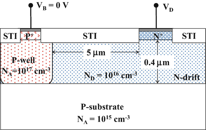
6.
At what drain voltage will avalanche breakdown occur in the structure below? Assume a critical field of 3 × 10⁵ V/cm and 25 °C.
-
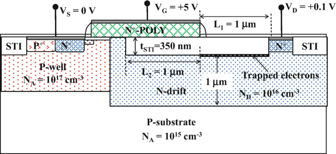
7.
The structure in the figure below was subjected to hot-electron stress during which electrons were trapped in the STI at the interface with the N-drift region. Assume that the trapped electrons are uniformly distributed at a concentration of 5 × 1011 cm−2. For 25 °C, estimate
-
(a)
The N-drift sheet resistance in the portion under the sheet of trapped electrons and under the portion covered by the poly gate
-
(b)
The drift resistance under the STI for a device width of 1 cm
-
(a)
-
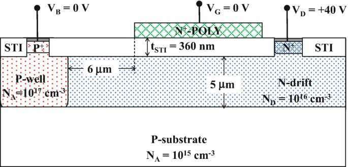
8.
Calculate the room temperature depletion width and the peak field in silicon in the N-drift region beneath the polysilicon plate, under the STI and at the N-drift-to-P-substrate junction shown in the figure below.
-
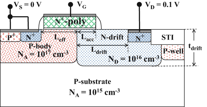
9.
For the planar NLDMOS in the figure below, assume Ldrift = 2 μm, Lacc = 0.5 μm, tdrift = 1.3 μm, Leff = 1.0 μm, Weff = 20 μm, tox = 15 nm, and no gate oxide charge. (a) Estimate the room temperature drift resistance for VG at flatband. (b) Estimate RDS(on) for VG = +5 V at 25 and 140 °C. Hint: for surface mobility, use the universal mobility plots in Chap. 6.
-
10.
Consider a 24-V NLDMOS power switch that should carry 10 A and must operate from −40 to +125 °C. The voltage drop across the structure may not exceed 0.5 V. The breakdown voltage, BVDSS, follows a normal distribution with σ = 0.5 V and has a temperature coefficient of 1500 ppm/°C. Assume 10% variation in the power supply voltage, 15% tolerant to RDS(on), and a device pitch of 3.25 μm. For a Six Sigma design, estimate the minimum width of the NLDMOS that should be designed to satisfy the above conditions.
-
11.
For an LDMOS of the type shown in Fig. 7.7, assume ND-drift = 5 × 1016 cm−3, tdrift = 1.5 μm, NA-body = 5 × 1016 cm−3, NA-SUB = 1015 cm−3, and no interaction with the MOS region. Determine
-
(a)
If this structure can achieve optimum RESURF (region II in Fig. 7.12)
-
(b)
The lateral (P-body/N-drift) breakdown voltage
-
(a)
-
12.
For the structure of the type in Fig. 7.7, determine the required P-substrate doping, Nsub, to achieve optimum RESURF assuming ND = 7 × 1016 cm−3 in the drift region and tdrift = 2 μm.
-
13.
The intrinsic MOSFET in an LDMOS is designed with tox = 12.5 nm, Leff = 0.6 μm, Weff = 10 μm, uniform body concentration NA = 2 × 1017 cm−3, and N+-poly gate. For VG = 5 V, at what temperature T will dID/dT ≈ 0?
-
14.
Explain why a MOSFET with a laterally graded channel as in NLDMOS exhibits a sharper peak in transconductance than a conventional NMOS having a laterally uniform channel.


Rights and permissions
Copyright information
© 2020 Springer Nature Switzerland AG
About this chapter

Cite this chapter
El-Kareh, B., Hutter, L.N. (2020). High-Voltage and Power Transistors. In: Silicon Analog Components. Springer, Cham. https://doi.org/10.1007/978-3-030-15085-3_7
Download citation
DOI: https://doi.org/10.1007/978-3-030-15085-3_7
Published:
Publisher Name: Springer, Cham
Print ISBN: 978-3-030-15084-6
Online ISBN: 978-3-030-15085-3
eBook Packages: EngineeringEngineering (R0)