
Abstract
Bipolar junction transistors (BJT) are inherent to CMOS technologies. Understanding the basic principles of operation of a BJT and its characteristics is not only important to efficiently use the component in bipolar and BiCMOS applications. It is also important to understand bipolar effects in CMOS, such as the subthreshold behavior, snapback, and latch-up, and to identify process and design techniques to modify their impact on circuit performance. Similarly, a discussion of integrated junction field-effect transistors (JFET) is important to its use in analog designs, mainly as a very low-noise, high input impedance device. It is also important to understand its parasitic effect, referred to as “the JFET effect” in high-voltage, high-power devices. The chapter begins with a review of BJT types, operation, and characteristics that are relevant to analog applications. This is followed by a description of JFET types, basic operation, and characteristics. The chapter concludes with simple circuit applications of both transistors.
This is a preview of subscription content, log in via an institution.
Buying options
Tax calculation will be finalised at checkout
Purchases are for personal use only
Learn about institutional subscriptionsNotes
- 1.
Recall that at ohmic contacts, carriers are at thermal equilibrium.
- 2.
hfe stands for hybrid model, small-signal forward-active mode, common emitter.
- 3.
Patterning, implanting, silicidation, and other unit processes are described in [2].
References
A.B. Phillips, Transistor Engineering (McGraw-Hill, 1962)
B. El-Kareh, Fundamentals of Semiconductor Processing Technologies (Kluwer Academic Publishers, 1995)
P.J. Coppen, W.T. Matzen, Distribution of recombination current in emitter-base junctions of silicon transistors. IEEE Trans. Electron Dev. ED-9(1), 75–81 (1962)
C.T. Sah, Effect of surface recombination and channel on p-n junction and transistor characteristics. IEEE Trans. Electron Dev. ED-9(1), 94–108 (1962)
C.T. Sah, R.N. Noyce, W. Shockley, Carrier generation and recombination in p-n junctions and p-n junction characteristics. IRE Trans. Electron Dev. 45(9), 1228–1238 (1957)
G.D. Mahan, Energy gap in Si and Ge: Impurity dependence. J. Appl. Phys. 51(5), 2634–2646 (1980)
T.N. Morgan, Broadening of impurity bands in heavily doped silicon. Phys. Rev. 139, 343–348 (1965)
R.J. Van Overstraeten, H.J. DeMan, R.P. Mertens, Transport equation in heavily doped silicon. IEEE Trans. Electron Dev. ED-20(3), 290–298 (1973)
H.P.D. Lanyon, R.A. Tuft, Bandgap narrowing in moderately to heavily doped silicon. IEEE Trans. Electron Dev. ED-26(7), 1014–1018 (1979)
J.W. Slotboom, H.C. DeGraaff, Bandgap narrowing in silicon bipolar transistors. IEEE Trans. Elecron Dev. ED-24(8), 1123–1125 (1977)
J. del Alamo, S. Swirhun, R.M. Swanson, Simultaneous measurement of hole lifetime, hole mobility and bandgap narrowing in heavily doped n-type silicon. IEEE IEDM Tech. Digest, 290–293 (1985)
E.J. McGrath, D.H. Navon, Factors limiting current gain in power transistors. IEEE Trans. Electron Dev. ED-24(10), 1255–1259 (1977)
B. El-Kareh, Chap. 3, in Silicon Devices and Process Integration, (Springer, 2009), p. 167
A. Hastings, The Art of Analog Layout (Pearson Prentice Hall, 2006), pp. 312–313
W.M. Webster, On the variation of junction transistor current amplification factor with emitter current. Proc. IRE 42(6), 914–920 (1954)
C.T. Kirk Jr., A theory of transistor cut-off frequency fall-off at high current densities. IEEE Trans Electron Dev. ED-9(2), 164–174 (1962)
S.K. Ghandhi, The Theory and Practice of Microelectronics (John Wiley and Sons, 1968)
Y.S. Yuan, Base current reversal in bipolar transistors and circuits: A review and update. IEE Proc.-Circuits Syst. 141(4), 299–306 (1994)
J.M. Early, Effects of space-charge layer widening in junction transistors. Proc. IRE 40, 1401–1406 (1952)
H.K. Gummel, A charge control relation for bipolar transistors. Bell Syst. Tech. J. 49, 115–120 (1970)
E.J. Prinz, J.C. Sturm, Analytical modeling of current gain – Early voltage products in Si/Si1-xGex/Si heterojunction bipolar transistors. IEEE IEDM Tech. Digest, 853–856 (1991)
L.J. Giacoletto, Study of p-n-p alloy junction transistor from d-c through medium frequencies. RCA Rev. 15(4), 506–562 (1954)
E.O. Johnson, Physical limitations on frequency and power parameters of transistors. RCA Rev., 163–177 (1975)
J. D. Cressler and G. Niu, Silicon-Germanium Heterojunction Bipolar Transistors., Artech House, 2003
T.H. Ning, D.D. Tang, Bipolar trends. Proc. IEEE 74(12), 1669–1677 (1986)
I. Getreu, Modeling the Bipolar Transistor (Tektronix Inc, 1976), p. 144
D.K. Schroder, Semiconductor Material Device Characterization (John Wiley and Sons, 1998), p. 218
R.J. Baker, CMOS, Design, Layout, and Simulation, J (Wiley & Sons, Inc., 2010)
P.R. Gray, P.J. Hurst, S.H. Lewis, R.G. Meyer, Analysis and Design of Analog Integrated Circuits (John Wiley & Sons, 2001)
D.F. Hilbiber, A new semiconductor voltage standard. IEEE ISSCC, Digest Tech. Papers, 32–33 (1964)
R.J. Widlar, New developments in IC voltage regulators. IEEE ISSCC, Digest Tech. Paper, 158–159 (1970)
A.P. Brokaw, A simple three-terminal IC bandgap reference. IEEE J. Solid State Circuits SC-9(6), 388–393 (1974)
C.R. Palmer, R.C. Dobkin, A Curvature Corrected Voltage Reference (ISSCC, 1981), pp. 58–59
G.C.M. Meijer, P.C. Schmale, K. van Zalinge, A new curvature corrected bandgap reference. IEEE JSSC SC-17(6), 1139–1143 (1982)
B.-S. Song, P.R. Gray, A precision curvature-compensated CMOS bandgap reference. IEEE JSSC SC-18(6), 634–643 (1983)
V.V. Ivanov, K.E. Sanborn, I.M. Filanovsky, Bandgap Voltage References with 1 V Supply (ESSCIRC, 2006), pp. 311–314
M.A.P. Pertijs, G.C.M. Meijer, J.H. Huijsing, Precision temperature measurement using CMOS substrate PNP transistors. IEEE Sensors J. 4(3), 294–300 m 2004
V.A. Vashchenko, D.J. LaFonteese, K.G. Korablev, Lateral PNP BJT ESD protection devices. IEEE BCTM, 53–56 (2008)
W. Shockley, A unipolar ‘field-effect’ transistor. Proc. IRE 40(11), 1367–1376 (1952)
Author information
Authors and Affiliations
Problems
Problems
The temperature is 300 K unless otherwise stated.
-
1.
In an NPN transistor operated in the forward-active mode, the base current is 10 nA and the emitter current 0.61 μA.
-
(a)
Neglect leakage current and find α and β.
-
(b)
The transistor is subjected to an accelerated aging stress, and β is found to drop to 29.5 at the same emitter current. Assume that β degradation is solely due increased emitter–base leakage after stress and calculate the leakage.
-
(a)
-
2.
An NPN transistor has a uniform total emitter area of 50 μm2. A forward voltage VBE = 0.7 V is applied to the base–emitter junction and a reverse voltage VCE = 5 V to the collector–base junction. The base and emitter currents are measured at, respectively, 1 and 61 μA. Assume low-level injection and determine:
-
(a)
The injection ratio
-
(b)
The emitter current density
-
(c)
The saturation current of the emitter–base junction
-
(d)
The collector current for a forward bias VBE = 0.75 V
-
(a)
-
3.
Show that the condition α1 + α2 > 1 is equivalent to β1 β2 > 1.
-
4.
The uniform doping concentrations in the emitter, base, and collector of an NPN transistor are, respectively, ND = 1020, NA = 2 × 10¹⁷, and ND = 8 × 1016 cm−3. The metallurgical base width is 0.8 μm and the emitter area is 10 μm2. The base–emitter junction is forward-biased at VBE = 0.6 V and the collector–base junction reversed-biased at 5 V.
-
(a)
Find the electrical base width Wb.
-
(b)
The minority electron concentration at the depletion boundary of the emitter–base junction.
-
(c)
The total charge of minority-carrier electrons in the base.
-
(a)
-
5.
The externally applied collector voltage in a grounded-emitter NPN is fixed at 1.5 V and the base–emitter junction gradually forward-biased. At VBE = 0.6 V, the collector current is 100 nA. For a total collector resistance of 1 kΩ, find VBE at the onset of saturation. Assume low-level injection and neglect emitter and base resistances.
-
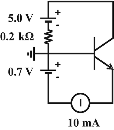
6.
Consider the NPN transistor in the following circuit. Neglect leakage currents.
-
(a)
Find the collector and base currents for α = 0.95.
-
(b)
Calculate the reverse voltage seen at the collector–base junction.
-
(a)
-
7.
The base and collector of an NPN transistor are uniformly doped at a concentration NA = ND = 2.5 × 1017 cm−3, and the emitter is degenerately doped. The distance between collector–base and emitter–base metallurgical junctions is 0.2 μm. The emitter is shorted to the base and the reverse collector voltage gradually increased. Will punch-through or avalanche breakdown occur first?
-
8.
Show that for a transistor in the forward-active mode, β is approximately proportional to the intrinsic base sheet resistance.
-
9.
A transistor is fabricated with an exponential base profile having a concentration of 5 × 1018 cm−3 at the emitter–base depletion boundary and 1017 cm−3 at the collector–base depletion boundary in the base. The base width Wb is 0.1 μm. For VCE = 1 V, VBE = 0.7 V calculate:
-
(a)
The base sheet resistance
-
(b)
The built-in field in the base
-
(c)
The minority-carrier drift velocity in the base
-
(d)
The base transit time
-
(a)
-
10.
In a PNP transistor, the collector current is kept constant, while the temperature is increased. IB decreases in magnitude, passes through zero, and changes polarity. What physical effects account for this behavior?
-
11.
Assume that an external resistor is placed in either the base lead or the emitter lead in a bipolar transistor of the type shown in Fig. 5.7. Which placement has the largest effect on the collector current IC?
-
12.
The emitter and base regions of an NPN transistor are uniformly doped with ND = 1018 cm−3 and NA = 1017 cm−3.
-
(a)
What are the thermal equilibrium minority and majority concentrations in the neutral regions?
-
(b)
Find the built-in voltage and depletion-layer width.
-
(c)
A forward voltage VBE = 0.6 V is applied to the junction. Neglect series resistances and find the excess electron and hole concentrations at the depletion edges of the emitter–base junction.
-
(d)
What are the percentile increases in the minority- and majority-carrier concentrations at those boundaries?
-
(e)
Repeat (c) and (d) for a forward voltage VBE = 0.82 V.
-
(a)
-
13.
Consider two N+P junctions formed at a distance 0.1 μm apart on a P-type substrate having a uniform concentration NA = 1015 cm−3. The electron lifetime in the P-type substrate is 10 μs.
-
(a)
Find the electron diffusion length in the substrate.
-
(b)
Do you expect this structure to exhibit bipolar action?
-
(c)
One of the junctions is forward-biased at VF = 0.6 V and the other reverse-biased at VR = 10 V.
-
(i)
Estimate the electron current density in the substrate.
-
(ii)
Calculate the excess electron current density in the substrate at the depletion edge of the forward-biased junction.
-
(iii)
Is the forward-biased junction in the high-level injection mode? Explain.
-
(i)
-
(a)
-
14.
In a PNP transistor, the emitter current is IE = 10 mA at VBE = 0.7 V.
-
(a)
Neglect series resistances and calculate the saturation current at 25 °C.
-
(b)
Calculate the absolute change and percentile changes in VF as IE is varied by ±75% from its initial value at 0.7 V.
-
(c)
Find the saturation current at 85 °C.
-
(a)
-
15.
The base width in an NPN transistor is 1.0 μm and the doping concentrations in the emitter, base, and collector are, respectively, ND = 1020, NA = 1 × 10¹⁶, and ND = 1017 cm−3. The emitter and base are shorted and the collector reverse-bias voltage increased. Will punch-through or avalanche breakdown occur first?
-
16.
In an NPN transistor operated in the forward-active mode, the emitter–base capacitance is CjE ≅ 2 fF, and the base width is Wb = 0.5 μm. The concentration in the base is 6 × 1017 cm−3. Assume that the unity-gain frequency fT is limited only by the emitter delay and base transit time, and estimate fT at IE = 1 μA and IE = 1 mA.
-
17.
Self-heating is the increase in transistor temperature during operation as a result of insufficient dissipation of power generated by the transistor. A transistor operates in the forward-active mode, and its temperature rises gradually as the collector voltage is increased.
-
(a)
For a constant VBE, how does the increase in temperature affect IC and IB?
-
(b)
How would VBE be affected if IB is kept constant as the temperature increases?
-
(a)
-
18.
The emitter–base junction xjE and collector–base junction xjC of an NPN transistor are, respectively, 0.45 and 0.71 μm deep. The emitter, base, and collector are uniformly doped with, respectively, ND = 1020 cm−3, NA = 1017 cm−3, and ND = 1017 cm−3. The base current density at VBE = 0.6 V is 3.23 × 10⁻³ A/cm2.
-
(a)
Estimate the NPN gain β at VCE = 1 V.
-
(b)
What is the maximum VCE that can be applied? What mechanism(s) limit this value?
-
(c)
Where would such a transistor be used?
-
(a)
-
19.
In a double-gated PJFET, the channel and gate concentrations are NA = 1016 cm−3 and ND = 1020 cm−3. Calculate the distance between the gate metallurgical junctions that will give a turn-off gate-to-source voltage VG = 1.4 V.
-
20.
In a double-gated NJFET, the channel and gate concentrations are ND = 1016 cm−3 and NA = 1020 cm−3. The channel depth is 2a = 0.4 μm. Is the transistor on or off at VG = 0?
-
21.
An NJFET is constructed on a P−-substrate which acts as a back gate and is held at ground. The doping concentrations in the channel, top gate, and substrate are, respectively, ND = 2.5 × 1016 cm−3, NA = 1020 cm−3, and NA = 1016 cm−3. The channel dimensions are a = 0.3 μm, W = 20 μm, and L = 10 μm.
-
(a)
Calculate the drain current for VG = 0 and VD = 0.1 V.
-
(b)
Find VDsat for the top-gate voltage VG = 0 and VG = −1 V.
-
(c)
At what top-gate voltage does the channel conductance gD to zero?
-
(a)
-
22.
In a symmetrical double-gated PJFET, the channel and gate concentrations are uniform with NA = 1016 cm−3 and ND = 1020 cm−3. The channel length, width, and metallurgical thickness are, respectively, 4 μm, 4 μm, and 0.76 μm. What gate voltage will yield a JFET resistance of 205 kΩ? Assume VD = 0.1 V and neglect source and drain series resistances.

Rights and permissions
Copyright information
© 2020 Springer Nature Switzerland AG
About this chapter

Cite this chapter
El-Kareh, B., Hutter, L.N. (2020). Bipolar and Junction Field-Effect Transistors. In: Silicon Analog Components. Springer, Cham. https://doi.org/10.1007/978-3-030-15085-3_5
Download citation
DOI: https://doi.org/10.1007/978-3-030-15085-3_5
Published:
Publisher Name: Springer, Cham
Print ISBN: 978-3-030-15084-6
Online ISBN: 978-3-030-15085-3
eBook Packages: EngineeringEngineering (R0)