
Abstract
This chapter focuses on methodologies for obtaining the so-called switched model. This model describes basic low-frequency dynamics, as given by the energy accumulation variations, and it captures the switching dynamics of power electronic converters as well.
Access this chapter
Tax calculation will be finalised at checkout
Purchases are for personal use only
References
Cellier F, Elmqvist H, Otter M (1996) Modeling from physical principles. In: Levine WS (ed) The control handbook. CRC Press/IEEE Press, Boca Raton, pp 99–107
Erikson RW, Maksimović D (2001) Fundamentals of power electronics, 2nd edn. Kluwer, Dordrecht, The Netherlands
Kassakian JG, Schlecht MF, Verghese GC (1991) Principles of power electronics. Addison-Wesley, Reading, Massachusetts
Krein PT, Bentsman J, Bass RM, Lesieutre B (1990) On the use of averaging for the analysis of power electronic systems. IEEE Trans Power Electron 5(2):182–190
Maksimović D, Stanković AM, Thottuvelil VJ, Verghese GC (2001) Modeling and simulation of power electronic converters. Proc IEEE 89(6):898–912
Malesani L, Rossetto L, Spiazzi G, Tenti P (1995) Performance optimization of Cúk converters by sliding-mode control. IEEE Trans Power Electron 10(3):302–309
Merdassi A, Gerbaud L, Bacha S (2010) Automatic generation of average models for power electronics systems in VHDL-AMS and modelica modelling languages. HyperSci J Model Simul Syst 1(3):176–186
Mohan N, Undeland TM, Robbins WP (2002) Power electronics: converters, applications and design, 3rd edn. Wiley, Hoboken
Sanders SR (1993) On limit cycles and the describing function method in periodically switched circuits. IEEE Trans Circuit Syst 40(9):564–572
Sanders SR, Verghese GC (1992) Lyapunov-based control for switched power converters. IEEE Trans Power Electron 7(1):17–24
Sun J, Grotstollen H (1992) Averaged modelling of switching power converters: reformulation and theoretical basis. In: Proceedings of the IEEE Power Electronics Specialists Conference – PESC 1992, Toledo, pp 1165–1172
Sun J, Mitchell DM, Greuel ME, Krein PT, Bass RM (1998) Modeling of PWM converters in discontinuous conduction mode – a reexamination. In: Proceedings of the 29th annual IEEE Power Electronics Specialists Conference – PESC 1998, Fukuoka, Japan, vol 1, pp 615–622
Tymerski R, Vorpérian V, Lee FCY, Baumann WT (1989) Nonlinear modelling of the PWM switch. IEEE Trans Power Electron 4(2):225–233
van Dijk E, Spruijt HJN, O’Sullivan DM, Klaassens JB (1995) PWM-switch modeling of DC-DC converters. IEEE Trans Power Electron 10(6):659–665
Vorpérian V (1990) Simplified analysis of PWM converters using model of PWM switch. Part II: discontinuous conduction mode. IEEE Trans Aerosp Electron Syst 26(3):497–505
Author information
Authors and Affiliations
Problems
Problems
Problem 3.1
In the example below, the Ćuk converter has been considered (see Fig. 3.17) where inductors L 1 and L 2 are not coupled. The switching function takes two values {0; 1}. Address the following points.

Electrical circuit of Ćuk DC-DC converter
-
(a)
Write the dynamical equations of the converter with respect to the switching function u.
-
(b)
Write the circuit model in the bilinear matrix form.
-
(c)
Draw the equivalent circuit of the converter and emphasize the coupling terms.
Solution
-
(a)
Let us take the current sense and voltage polarity as indicated in Fig. 3.17. Transistor H and diode D form the switching network; a single switching function u feeds the transistor gate. When u = 1, switch H is turned on and D is polarized inversely, leading to the configuration depicted in Fig. 3.18a. As u = 0, H turns off, diode D enters into conduction and the second configuration is shown in Fig. 3.18b.
Fig. 3.18 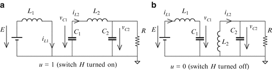
The two possible configurations of the Cúk converter
Kirchhoff’s laws for the two topologies give
$$ \begin{array}{ll}u=1:\left\{\begin{array}{l}\overset{\cdotp }{i_{L1}}=E/{L}_1\\ {}\overset{\cdotp }{v_{C1}}={i}_{L2}/{C}_1\\ {}\overset{\cdotp }{i_{L2}}=-{v}_{C1}/{L}_2-{v}_{C2}/{L}_2\\ {}\overset{\cdotp }{v_{C2}}={i}_{L2}/{C}_2-{v}_{C2}/(RC),\end{array}\right.\hfill & u=0:\left\{\begin{array}{l}\overset{\cdotp }{i_{L1}}=E/{L}_1-{v}_{C1}/{L}_1\\ {}\overset{\cdotp }{v_{C1}}={i}_{L1}/{C}_1\\ {}\overset{\cdotp }{i_{L2}}=-{v}_{C2}/{L}_2\\ {}\overset{\cdotp }{v_{C2}}={i}_{L2}/{C}_2-{v}_{C2}/\left(R{C}_2\right).\end{array}\right.\hfill \end{array} $$By multiplying the two sets of equations with u and (1–u), respectively, and summing, one obtains
$$ \left\{\begin{array}{l}\overset{\cdotp }{i_{L1}}=-\left(1-u\right)\cdot {v}_{C1}/{L}_1+E/{L}_1\hfill \\ {}\overset{\cdotp }{v_{C1}}=\left(1-u\right)\cdot {i}_{L1}/{C}_1+u\cdot {i}_{L2}/{C}_1\hfill \\ {}\overset{\cdotp }{i_{L2}}=-u\cdot {v}_{C1}/{L}_2-{v}_{C2}/{L}_2\hfill \\ {}\overset{\cdotp }{v_{C2}}={i}_{L2}/{C}_2-{v}_{C2}/\left(R{C}_2\right).\hfill \end{array}\right. $$(3.20) -
(b)
By denoting by \( \mathbf{x}={\left[\begin{array}{cccc}\hfill {i}_{L1}\hfill & \hfill {v}_{C1}\hfill & \hfill {i}_{L2}\hfill & \hfill {v}_{C2}\hfill \end{array}\right]}^T \) the state vector (each of its components describes an energy accumulation), the set of Eq. (3.20) can be rewritten in matrix form as
$$ \overset{\cdotp }{\mathbf{x}}=\left[\begin{array}{cccc}\hfill 0\hfill & \hfill -1/{L}_1\hfill & \hfill 0\hfill & \hfill 0\hfill \\ {}\hfill 1/{C}_1\hfill & \hfill 0\hfill & \hfill 0\hfill & \hfill 0\hfill \\ {}\hfill 0\hfill & \hfill 0\hfill & \hfill 0\hfill & \hfill -1/{L}_2\hfill \\ {}\hfill 0\hfill & \hfill 1/{C}_2\hfill & \hfill 0\hfill & \hfill -1/\left(R{C}_2\right)\hfill \end{array}\right]\cdot \mathbf{x}+\left[\begin{array}{c}\hfill u\cdot {v}_{C1}/{L}_1\hfill \\ {}\hfill u\cdot {i}_{L1}/{C}_1+u\cdot {i}_{L2}/{C}_1\hfill \\ {}\hfill -u\cdot {v}_{C1}/{L}_2\hfill \\ {}\hfill 0\hfill \end{array}\right]+\left[\begin{array}{c}\hfill E/{L}_1\hfill \\ {}\hfill 0\hfill \\ {}\hfill 0\hfill \\ {}\hfill 0\hfill \end{array}\right]. $$

Note that there is a single switching function, therefore p = 1. By processing the second term of the above matrix relation, one obtains
with
Equations (3.20) lead to the equivalent circuit in Fig. 3.19. The first equation of (3.20) gives the first circuit, where the dependent voltage source is a function of the inductor current in the second circuit. The second equation gives the second circuit. Note that the two dependent current sources are coupled with variables from the other two circuits (the inductor current from the first circuit and the capacitor voltage from the third one). These coupled sources can be seen as variable-ratio DC ideal transformers. The third circuit is the image of the last two equations in (3.19).

Equivalent circuit of switched model of Cúk converter, presented in Fig. 3.17
Problem 3.2
Let consider the half-bridge voltage inverter (current rectifier) of Fig. 3.20. Switching function u is defined to take the value 1 if switch F 1 is turned on and the value −1 if switch F 2 is turned on. Zero indices concern continuous variables, whereas indices a concern alternative variables.

Half-bridge voltage inverter
-
(a)
Write the system equations by making appear the switching function u.
-
(b)
Prove that the switched model of the system may be represented by the equivalent circuit from Fig. 3.21.
Fig. 3.21 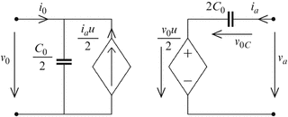
Equivalent topologic diagram of inverter from Fig. 3.20

Solution
The evolution of the filtering capacitor voltages is given by
The expression of the alternative voltage is \( {v}_a=\frac{1+u}{2}\cdot {v}_{01}+\frac{1-u}{2}\cdot {v}_{02} \). Taking v 0c = (v 01 + v 02)/2 and knowing that v 0 = v 01 − v 02 one obtains
Equation (3.21) allows the equivalent circuit of Fig. 3.21 to be built as representation of the switched model. This proof is useful for solving Problem 3.3.
The following problems are left to the reader to solve.
Problem 3.3
Current-source inverter
Let us consider the half-bridge current source inverter presented in Fig. 3.22. Prove that the equivalent diagram shown in Fig. 3.23 corresponds to the circuit given in Fig. 3.22.

Half-bridge current source inverter

Equivalent topological diagram of current source inverter from Fig. 3.22
Problem 3.4
Series-resonance power supply
Let us consider the converter given in Fig. 3.24. Switching functions u 1 and u 2 are such that

Series-resonance voltage power supply based on capacitive half-bridges
-
(a)
Write the observable state model of the system, i.e., of appropriate order, and prove that for this model the equivalent circuit is the one shown in Fig. 3.25.
Fig. 3.25 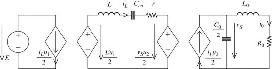
The equivalent topologic diagram of the converter in Fig. 3.24
-
(b)
Find out the value of capacitor C eq from the equivalent circuit.

Problem 3.5
Buck-boost power stage
Consider the DC-DC converter given in Fig. 3.26.

Buck-boost DC-DC converter
-
(a)
Establish the switched model of converter in Fig. 3.26 by considering a switching function that takes its values in the set {0;1}, namely, value 1 corresponds to switch H being turned on and value 0 to the same switch being turned off.
-
(b)
Identify the variables switched by power switches H and D.
-
(c)
Draw the equivalent diagram.
Problem 3.6
Zeta DC-DC power stage
-
(a)
Deduce the switched model of the DC-DC converter from Fig. 3.27 by considering a switching function that takes value 1 when switch H is turned on and value 0 when the same switch is turned off. Consider the voltage polarity and current sense as indicated in Fig. 3.27.
Fig. 3.27 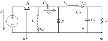
Zeta DC-DC converter
-
(b)
Identify the variables switched by power switches H and D.
-
(c)
Draw the equivalent diagram.

Rights and permissions
Copyright information
© 2014 Springer-Verlag London
About this chapter
Cite this chapter
Bacha, S., Munteanu, I., Bratcu, A.I. (2014). Switched Model. In: Power Electronic Converters Modeling and Control. Advanced Textbooks in Control and Signal Processing. Springer, London. https://doi.org/10.1007/978-1-4471-5478-5_3
Download citation
DOI: https://doi.org/10.1007/978-1-4471-5478-5_3
Published:
Publisher Name: Springer, London
Print ISBN: 978-1-4471-5477-8
Online ISBN: 978-1-4471-5478-5
eBook Packages: EngineeringEngineering (R0)