
Abstract
The emergence of different fabrication techniques of silicon nanowires (SiNWs) raises the question of finding a suitable architectural organization of circuits based on them. Despite the possibility of building conventional CMOS circuits with SiNWs, the ability to arrange them into regular arrays, called crossbars, offers the opportunity to achieve higher integration densities. In such arrays, molecular switches or phase-change materials are grafted at the crosspoints, i.e., the crossing nanowires, in order to perform computation or storage. Given the fact that the technology is not mature, a hybridization of CMOS circuits with nanowire arrays seems to be the most promising approach.
This is a preview of subscription content, log in via an institution.
Buying options
Tax calculation will be finalised at checkout
Purchases are for personal use only
Learn about institutional subscriptionsNotes
- 1.
The authors would like to acknowledge those who contributed to [1].
- 2.
If we consider short-channel transistors, then the saturation current is proportional to (VA,i − V th) and δ = (α + υ)/q.
References
M. H. Ben Jamaa, “Fabrication and Design of Nanoscale Regular Circuits,” PhD Thesis at Ecole Polytechnique Fédérale de Lausanne (EPFL), Sept. 2010.
R. S. Wagner and W. C. Ellis, “Vapor-liquid-solid mechanism for single crystal growth,” Applied Physics Letters, vol. 4, no. 5, pp. 89–90, 1964.
Y. Cui, X. Duan, J. Hu, and C. M. Lieber, “Doping and electrical transport in silicon nanowires,” The Journal of Physical Chemistry B, vol. 4, no. 22, pp. 5213–5216, 2000.
R. He and P. Yang, “Giant piezoresistance effect in silicon nanowires,” Nature Nanotechnology, vol. 1, no. 1, pp. 42–46, 2006.
L. J. Lauhon, M. S. Gudiksen, D. Wang, and C. M. Lieber, “Epitaxial core-shell and core-multishell nanowire heterostructures,” Nature, vol. 420, pp. 57–61, 2002.
K. E. Moselund, D. Bouvet, L. Tschuor, V. Pot, P. Dainesi, C. Eggimann, N. L. Thomas, R. Houdré, and A. M. Ionescu, “Cointegration of gate-all-around MOSFETs and local silicon-on-insulator optical waveguides on bulk silicon,” IEEE Transactions on Nanotechnology, vol. 6, no. 1, pp. 118–125, 2007.
K.-N. Lee, S.-W. Jung, W.-H. Kim, M.-H. Lee, K.-S. Shin, and W.-K. Seong, “Well controlled assembly of silicon nanowires by nanowire transfer method,” Nanotechnology, vol. 18, no. 44, p. 445302 (7pp), 2007.
S. D. Suk, S.-Y. Lee, S.-M. Kim, E.-J. Yoon, M.-S. Kim, M. Li, C. W. Oh, K. H. Yeo, S. H. Kim, D.-S. Shin, K.-H. Lee, H. S. Park, J. N. Han, C. Park, J.-B. Park, D.-W. Kim, D. Park, and B.-I. Ryu, “High performance 5nm radius twin silicon nanowire MOSFET (TSNWFET): fabrication on bulk Si wafer, characteristics, and reliability,” in Proc. IEEE Int. Electron Devices Meeting, pp. 717–720, Dec. 2005.
D. Sacchetto, M. H. Ben-Jamaa, G. De Micheli, and Y. Leblebici, “Fabrication and characterization of vertically stacked gate-all-around Si nanowire FET arrays,” in Proc. European Solid-State Device Research Conference, 2009.
L. Doherty, H. Liu, and V. Milanovic, “Application of MEMS technologies to nanodevices,” Circuits and Systems, 2003. ISCAS ’03. Proceedings of the 2003 International Symposium on, vol. 3, pp. III–934–III–937, May 2003.
R. M. Y. Ng, T. Wang, and M. Chan, “A new approach to fabricate vertically stacked single-crystalline silicon nanowires,” in Proc. IEEE Conf. on Electron Devices and Solid-State Circuits, pp. 133–136, Dec. 2007.
S.-M. Koo, A. Fujiwara, J.-P. Han, E. M. Vogel, C. A. Richter, and J. E. Bonevich, “High inversion current in silicon nanowire field effect transistors,” Nano Letters, vol. 4, no. 11, pp. 2197–2201, 2004.
J. Kedzierski and J. Bokor, “Fabrication of planar silicon nanowires on silicon-on-insulator using stress limited oxidation,” Journal of Vacuum Science and Technology B, vol. 15, no. 6, pp. 2825–2828, 1997.
V. Auzelyte, H. H. Solak, Y. Ekinci, R. MacKenzie, J. Vrs, S. Olliges, and R. Spolenak, “Large area arrays of metal nanowires,” Microelectronic Engineering, vol. 85, no. 5–6, pp. 1131–1134, 2008.
O. Vazquez-Mena, G. Villanueva, V. Savu, K. Sidler, M. A. F. van den Boogaart, and J. Brugger, “Metallic nanowires by full wafer stencil lithography,” Nano Letters, vol. 8, no. 11, pp. 3675–3682, 2008.
J. Hållstedt, P.-E. Hellström, Z. Zhang, B. Malm, J. Edholm, J. Lu, S.-L. Zhang, H. Radamson, and M. Östling, “A robust spacer gate process for deca-nanometer high-frequency MOSFETs,” Microelectronic Engineering, vol. 83, no. 3, pp. 434–439, 2006.
Y.-K. Choi, J. S. Lee, J. Zhu, G. A. Somorjai, L. P. Lee, and J. Bokor, “Sublithographic nanofabrication technology for nanocatalysts and DNA chips,” Journal of Vacuum Science Technology B: Microelectronics and Nanometer Structures, vol. 21, pp. 2951–2955, 2003.
W. Wu, G.-Y. Jung, D. L. Olynick, J. Straznicky, Z. Li, X. Li, D. A. A. Ohlberg, Y. Chen, S.-Y. Wang, J. A. Liddle, W. M. Tong, and R. S. Williams, “One-kilobit cross-bar molecular memory circuits at 30-nm half-pitch fabricated by nanoimprint lithography,” Applied Physics A: Materials Science and Processing, vol. 80, no. 6, pp. 1173–1178, 2005.
G.-Y. Jung, E. Johnston-Halperin, W. Wu, Z. Yu, S.-Y. Wang, W. M. Tong, Z. Li, J. E. Green, B. A. Sheriff, A. Boukai, Y. Bunimovich, J. R. Heath, and R. S. Williams, “Circuit fabrication at 17 nm half-pitch by nanoimprint lithography,” Nano Letters, vol. 6, no. 3, pp. 351–354, 2006.
Y. Huang, X. Duan, Q. Wei, and C. M. Lieber, “Directed assembly of one-dimensional nanostructures into functional networks,” Science, vol. 291, no. 5504, pp. 630–633, 2001.
P. A. Smith, C. D. Nordquist, T. N. Jackson, T. S. Mayer, B. R. Martin, J. Mbindyo, and T. E. Mallouk, “Electric-field assisted assembly and alignment of metallic nanowires,” Applied Physics Letters, vol. 77, pp. 1399–1401, 2000.
X. Duan, Y. Huang, Y. Cui, J. Wang, and C. M. Lieber, “Indium phosphide nanowires as building blocks for nanoscale electronic and optoelectronic devices,” Nature, vol. 409, pp. 66–69, 2001.
Y. Chen, D. A. A. Ohlberg, X. Li, D. R. Stewart, R. Stanley Williams, J. O. Jeppesen, K. A. Nielsen, J. F. Stoddart, D. L. Olynick, and E. Anderson, “Nanoscale molecular-switch devices fabricated by imprint lithography,” Applied Physics Letters, vol. 82, pp. 1610–1612, 2003.
J. A. Zasadzinski, R. Viswanathan, L. Madsen, J. Garnaes, and D. K. Schwartz, “Langmuir-Blodgett films,” Science, vol. 263, no. 5154, pp. 1726–1733, 1994.
N. A. Melosh, A. Boukai, F. Diana, B. Gerardot, A. Badolato, P. M. Petroff, and J. R. Heath, “Ultrahigh-density nanowire lattices and circuits,” Science, vol. 300, no. 5616, pp. 112–115, 2003.
J. E. Green, J. W. Choi, A. Boukai, Y. Bunimovich, E. Johnston-Halperin, E. Deionno, Y. Luo, B. A. Sheriff, K. Xu, Y. S. Shin, H.-R. Tseng, J. F. Stoddart, and J. R. Heath, “A 160-kilobit molecular electronic memory patterned at 1011 bits per square centimetre,” Nature, vol. 445, pp. 414–417, 2007.
G. Ho, J. R. Heath, M. Kondratenko, D. F. Perepichka, K. Arseneault, M. Pézolet, and M. R. Bryce, “The first studies of a tetrathiafulvalene-sigma-acceptor molecular rectifier,” Chemistry – A European Journal, vol. 11, no. 10, pp. 2914–2922, 2005.
R. L. McCreery, “Molecular electronic junctions,” Chemistry of Materials, vol. 16, no. 23, pp. 4477–4496, 2004.
G. J. Ashwell, B. Urasinska, and W. D. Tyrrell, “Molecules that mimic Schottky diodes,” Physical Chemistry Chemical Physics (Incorporating Faraday Transactions), vol. 8, pp. 3314–3319, 2006.
Y. Luo, C. P. Collier, J. O. Jeppesen, K. A. Nielsen, E. DeIonno, G. Ho, J. Perkins, H.-R. Tseng, T. Yamamoto, J. F. Stoddart, and J. R. Heath, “Two-dimensional molecular electronics circuits,” Journal of Chemical Physics and Physical Chemistry, vol. 3, pp. 519–525, 2002.
C. P. Collier, G. Mattersteig, E. W. Wong, Y. Luo, K. Beverly, J. Sampaio, F. M. Raymo, J. F. Stoddart, and J. R. Heath, “A [2]catenane-based solid state electronically reconfigurable switch,” Science, vol. 289, pp. 1172–1175, 2000.
Y. Zhang, S. Kim, J. McVittie, H. Jagannathan, J. Ratchford, C. Chidsey, Y. Nishi, and H.-S. Wong, “An integrated phase change memory cell with Ge nanowire diode for cross-point memory,” in Proc. IEEE Symp. on VLSI Technology, pp. 98–99, June 2007.
A. DeHon, “Design of programmable interconnect for sublithographic programmable logic arrays,” in Proc. Int. Symp. on Field-Programmable Gate Arrays, 2005, pp. 127–137.
W. Culbertson, R. Amerson, R. Carter, P. Kuekes, and G. Snider, “Defect tolerance on the Teramac custom computer,” in Proc. IEEE Symp. on FPGAs for Custom Computing Machines, pp. 116–123, Apr. 1997.
J. R. Heath, P. J. Kuekes, G. S. Snider, and R. S. Williams, “A defect-tolerant computer architecture: Opportunities for nanotechnology,” Science, vol. 280, no. 5370, pp. 1716–1721.
S. C. Goldstein and M. Budiu, “NanoFabrics: Spatial computing using molecular electronics,” in Proc. Int. Symp. on Computer Architecture, 2001, pp. 178–189.
S. Goldstein and D. Rosewater, “Digital logic using molecular electronics,” in Proc. IEEE Int. Solid-State Circuits Conference, vol. 1, pp. 204–459, 2002.
M. S. Gudiksen, L. J. Lauhon, J. Wang, D. C. Smith, and C. M. Lieber, “Growth of nanowire superlattice structures for nanoscale photonics and electronics,” Nature, vol. 415, pp. 617–620, 2002.
A. DeHon and K. K. Likharev, “Hybrid CMOS/nanoelectronic digital circuits: devices, architectures, and design automation,” in Proc. IEEE/ACM Int. Conf. on Computer-aided Design, 2005, pp. 375–382.
A. DeHon, P. Lincoln, and J. Savage, “Stochastic assembly of sublithographic nanoscale interfaces,” IEEE Trans. on Nanotechnology, vol. 2, no. 3, pp. 165–174, 2003.
J. E. Savage, E. Rachlin, A. DeHon, C. M. Lieber, and Y. Wu, “Radial addressing of nanowires,” ACM Journal on Emerging Technologies in Computing Systems, vol. 2, no. 2, pp. 129–154, 2006.
R. Beckman, E. Johnston-Halperin, Y. Luo, J. E. Green, and J. R. Heath, “Bridging dimensions: demultiplexing ultrahigh density nanowire circuits,” Science, vol. 310, no. 5747, pp. 465–468, 2005.
P. J. Kuekes and R. S. Williams, “Demultiplexer for a molecular wire crossbar network (MWCN DEMUX),” US Patent 6,256,767, 2001.
T. Hogg, Y. Chen, and P. Kuekes, “Assembling nanoscale circuits with randomized connections,” IEEE Trans. on Nanotechnology, vol. 5, no. 2, pp. 110–122, 2006.
E. Rachlin, “Robust nanowire decoding,” 2006. [Online]. Available: http://www.cs.brown.edu/publications/theses/masters/2006/eerac.pdf
D. A. Anderson and G. Metze, “Design of totally self-checking check circuits for m-out of-n codes,” in Proc. Int. Symp. on Fault-Tolerant Computing, "Highlights from Twenty-Five Years,” pp. 244–248, June 1995.
M. H. Ben Jamaa, D. Atienza, K. E. Moselund, D. Bouvet, A. M. Ionescu, Y. Leblebici, and G. De Micheli, “Variability-aware design of multilevel logic decoders for nanoscale crossbar memories,” IEEE Trans. on Computer-Aided Design, vol. 27, no. 11, pp. 2053–2067, Nov. 2008.
R. K. Brayton, Sensitivity and Optimization. Elsevier, 1980.
J. M. Rabaey, Digital Integrated Circuits: A Design Perspective. Prentice-Hall International Editions, 1996.
C. F. Cerofolini, “The multi-spacer patterning technique: a non-lithographic technique for terascale integration,” Semiconductor Science and Technology, 23(2008) 075020.
Author information
Authors and Affiliations
Corresponding author
Editor information
Editors and Affiliations
Appendices
Exercise 1 Delay in a Crossbar
Consider the following NxN crossbar circuit with N nanowires in every plane and M = log2(N) access transistors in the decoder of every plane. Determine the delay through the crossbar when the address corrsponding to the crosspoint (X,Y) is activated (X and Y are between 1 and M). Assume the following parameters:
-
Decoder parameters:
-
On-resistance of an access transistor: Ron = 10 kΩ
-
Off-resistance of an access transistor: Roff = 100 MΩ
-
Drain/source capacitances of an access transistor: CD/S = 1 fF
-
-
Parameters of the functional part of the crossbar
-
Resistance of a nanowire length unit equal to the nanowire pitch: RNW = 100 Ω
-
Capacitance of a molecular switch: CS = 2 fF
-
Resistance through a molecular switch: RS = 1 kΩ
-
Parasistic capacitance between crossing nanowires, parallel nanowires and between the nanowires and the substrate: not included
Ex. Figure 1 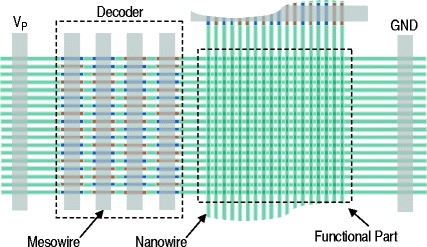
Baseline crossbar architecture
-

Exercise 2 Process Optimization
In goal of this exercise is to optimize the geometry of mask used in the MSPT process. The MSPT can used iteratively, starting with a given sacrificial layer, in order to define the spacers that may be used as sacrifical layers in the following steps.
This techniques envolves the deposition of a first sacrificial layer (1st step) with the width W and pitch P. Then, a sacrificial layer with the height W1 = qW is deposited (2nd step) and etched (3rd step) in order the form the sacrifical layer with the width W1 and a smaller pitch than P (4th step). These steps can be repeated with a following deposition of a layer with a height W2 = q W1 (step 5 to 7) in order to decrease the pitch further.
Questions taken from [50]:
-
1
Calculate the extension of the spacer underneath and beyond the first sacrificial layer after n iterations (lout(n) and lin(n) respectively).
-
2
For a large number of iterations, calculate the optimal values for q and W/P.
Ex. Figure 2 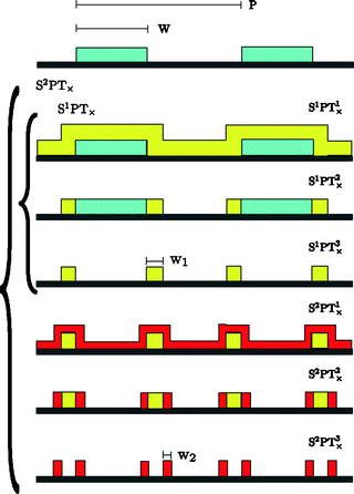
Multiplicative road of the multi-spacer technique [50]

Rights and permissions
Copyright information
© 2011 Springer Science+Business Media, LLC
About this chapter
Cite this chapter
Jamaa, M.H.B., De Micheli, G. (2011). Reliable Circuits Design with Nanowire Arrays. In: Jha, N., Chen, D. (eds) Nanoelectronic Circuit Design. Springer, New York, NY. https://doi.org/10.1007/978-1-4419-7609-3_5
Download citation
DOI: https://doi.org/10.1007/978-1-4419-7609-3_5
Published:
Publisher Name: Springer, New York, NY
Print ISBN: 978-1-4419-7444-0
Online ISBN: 978-1-4419-7609-3
eBook Packages: EngineeringEngineering (R0)