Abstract
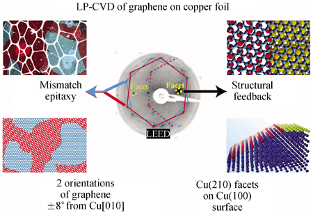
Graphene growth by low-pressure chemical vapor deposition on low cost copper foils shows great promise for large scale applications. It is known that the local crystallography of the foil influences the graphene growth rate. Here we find an epitaxial relationship between graphene and copper foil. Interfacial restructuring between graphene and copper drives the formation of (n10) facets on what is otherwise a mostly Cu(100) surface, and the facets in turn influence the graphene orientations from the onset of growth. Angle resolved photoemission shows that the electronic structure of the graphene is decoupled from the copper indicating a weak interaction between them. Despite this, two preferred orientations of graphene are found, ±8° from the Cu[010] direction, creating a non-uniform distribution of graphene grain boundary misorientation angles. Comparison with the model system of graphene growth on single crystal Cu(110) indicates that this orientational alignment is due to mismatch epitaxy. Despite the differences in symmetry the orientation of the graphene is defined by that of the copper. We expect these observations to not only have importance for controlling and understanding the growth process for graphene on copper, but also to have wider implications for the growth of two-dimensional materials on low cost metal substrates.

Article PDF
References
Li, X.; Cai, W.; An, J.; Kim, S.; Nah, J.; Yang, D.; Piner, R.; Velamakanni, A.; Jung, I.; Tutuc, E., et al. Large-area synthesis of high-quality and uniform graphene films on copper foils. Science 2009, 324, 1312–1314.
Huang, P. Y.; Ruiz-Vargas, C. S.; van der Zande, A. M.; Whitney, W. S.; Levendorf, M. P.; Kevek, J. W.; Garg, S.; Alden, J. S.; Hustedt, C. J.; Zhu, Y., et al. Grains and grain boundaries in single-layer graphene atomic patchwork quilts. Nature 2011, 469, 389–392.
An, J.; Voelkl, E.; Suk, J. W.; Li, X.; Magnuson, C. W.; Fu, L.; Tiemeijer, P.; Bischoff, M.; Freitag, B.; Popova, E., et al. Domain (grain) boundaries and evidence of “twinlike” structures in chemically vapor deposited grown graphene. ACS Nano 2011, 5, 2433–2439.
Kim, K.; Lee, Z.; Regan, W.; Kisielowski, C.; Crommie, M. F.; Zettl, A. Grain boundary mapping in polycrystalline graphene. ACS Nano 2011, 5, 2142–2146.
Yakobson, B. I.; Ding, F. Observational geology of graphene, at the nanoscale. ACS Nano 2011, 5, 1569–1574.
Yu, Q.; Jauregui, L. A.; Wu, W.; Colby, R.; Tian, J.; Su, Z.; Cao, H.; Liu, Z.; Pandey, D.; Wei, D., et al. Control and characterization of individual grains and grain boundaries in graphene grown by chemical vapour deposition. Nat. Mater. 2011, 10, 443–449.
Malola, S.; Häkkinen, H.; Koskinen, P. Structural, chemical, and dynamical trends in graphene grain boundaries. Phys. Rev. B 2010, 81, 165447.
Zhang, J.; Zhao, J.; Lu, J. Intrinsic strength and failure behaviors of graphene grain boundaries. ACS Nano 2012, 6, 2704–2711.
Grantab, R.; Shenoy, V. B.; Ruoff, R. S. Anomalous strength characteristics of tilt grain boundaries in graphene. Science 2010, 330, 946–948.
Kumar, S. B.; Guo, J. Strain-induced conductance modulation in graphene grain boundary. Nano Lett. 2012, 12, 1362–1366.
Wintterlin, J.; Bocquet, M. L. Graphene on metal surfaces. Surf. Sci. 2009, 603, 1841–1852.
Robinson, Z. R.; Tyagi, P.; Murray, T. M.; Ventrice, J. C. A.; Chen, S.; Munson, A.; Magnuson, C. W.; Ruoff, R. S. Substrate grain size and orientation of Cu and Cu-Ni foils used for the growth of graphene films. J. Vac. Sci. Technol. A 2012, 30, 011401.
Chen, S.; Cai, W.; Piner, R. D.; Suk, J. W.; Wu, Y.; Ren, Y.; Kang, J.; Ruoff, R. S. Synthesis and characterization of large-area graphene and graphite films on commercial Cu-Ni alloy foils. Nano Lett. 2011, 11, 3519–3525.
Ishihara, M.; Koga, Y.; Kim, J.; Tsugawa, K.; Hasegawa, M. Direct evidence of advantage of Cu(111) for graphene synthesis by using Raman mapping and electron backscatter diffraction. Mater. Lett. 2011, 65, 2864–2867.
Wood, J. D.; Schmucker, S. W.; Lyons, A. S.; Pop, E.; Lyding, J. W. Effects of polycrystalline Cu substrate on graphene growth by chemical vapor deposition. Nano Lett. 2011, 11, 4547–4554.
Nie, S.; Wofford, J. M.; Bartelt, N. C.; Dubon, O. D.; McCarty, K. F. Origin of the mosaicity in graphene grown on Cu(111). Phys. Rev. B 2011, 84, 155425.
Zhao, L.; Rim, K. T.; Zhou, H.; He, R.; Heinz, T. F.; Pinczuk, A.; Flynn, G. W.; Pasupathy, A. N. Influence of copper crystal surface on the CVD growth of large area monolayer graphene. Solid State Commun. 2011, 151, 509–513.
Gao, L.; Guest, J. R.; Guisinger, N. P. Epitaxial graphene on Cu(111). Nano Lett. 2010, 10, 3512–3516.
Ogawa, Y.; Hu, B.; Orofeo, C. M.; Tsuji, M.; Ikeda, K.-i.; Mizuno, S.; Hibino, H.; Ago, H. Domain structure and boundary in single-layer graphene grown on Cu(111) and Cu(100) Films. J. Phys. Chem. Lett. 2011, 3, 219–226.
Orofeo, C. M.; Hibino, H.; Kawahara, K.; Ogawa, Y.; Tsuji, M.; Ikeda, K.-I.; Mizuno, S.; Ago, H. Influence of Cu metal on the domain structure and carrier mobility in single-layer graphene. Carbon 2012, 50, 2189–2196.
Wofford, J. M.; Nie, S.; McCarty, K. F.; Bartelt, N. C.; Dubon, O. D. Graphene islands on Cu foils: The interplay between shape, orientation, and defects. Nano Lett. 2010, 10, 4890–4896.
Rasool, H. I.; Song, E. B.; Allen, M. J.; Wassei, J. K.; Kaner, R. B.; Wang, K. L.; Weiller, B. H.; Gimzewski, J. K. Continuity of graphene on polycrystalline copper. Nano Lett. 2010, 11, 251–256.
Zhang, B.; Lee, W. H.; Piner, R.; Kholmanov, I.; Wu, Y.; Li, H.; Ji, H.; Ruoff, R. S. Low-temperature chemical vapor deposition growth of graphene from toluene on electropolished copper foils. ACS Nano 2012, 6, 2471–2476.
Lee, C.; Li, Q.; Kalb, W.; Liu, X.-Z.; Berger, H.; Carpick, R. W.; Hone, J. Frictional characteristics of atomically thin sheets. Science 2010, 328, 76–80.
Tian, J.; Cao, H.; Wu, W.; Yu, Q.; Guisinger, N. P.; Chen, Y. P. Graphene induced surface reconstruction of Cu. Nano Lett. 2012, 12, 3893–3899.
Khomyakov, P. A.; Giovannetti, G.; Rusu, P. C.; Brocks, G.; van den Brink, J.; Kelly, P. J. First-principles study of the interaction and charge transfer between graphene and metals. Phys. Rev. B 2009, 79, 195425.
Walter, A. L.; Nie, S.; Bostwick, A.; Kim, K. S.; Moreschini, L.; Chang, Y. J.; Innocenti, D.; Horn, K.; McCarty, K. F.; Rotenberg, E. Electronic structure of graphene on single-crystal copper substrates. Phys. Rev. B 2011, 84, 195443.
Gartland, P. O.; Berge, S.; Slagsvold, B. J. Photoelectric work function of a copper single crystal for the (100), (110), (111), and (112) faces. Phys. Rev. Lett. 1972, 28, 738–739.
Castro Neto, A. H.; Guinea, F.; Peres, N. M. R.; Novoselov, K. S.; Geim, A. K. The electronic properties of graphene. Rev. Mod. Phys. 2009, 81, 109–162.
Quigley, D.; Rodger, P. M.; Freeman, C. L.; Harding, J. H.; Duffy, D. M. Metadynamics simulations of calcite crystallization on self-assembled monolayers. J. Chem. Phys. 2009, 131, 094703.
Fölsch, S.; Helms, A.; Zöphel, S.; Repp, J.; Meyer, G.; Rieder, K. H. Self-organized patterning of an insulator-on-metal system by surface faceting and selective growth: NaCl/Cu(211). Phys. Rev. Lett. 2000, 84, 123–126.
Murray, P. W.; Pedersen, M. Ø.; Lægsgaard, E.; Stensgaard, I.; Besenbacher, F. Growth of C60 on Cu(110) and Ni(110) surfaces: C60-induced interfacial roughening. Phys. Rev. B 1997, 55, 9360–9363.
Gao, J.; Yip, J.; Zhao, J.; Yakobson, B. I.; Ding, F. Graphene nucleation on transition metal surface: Structure transformation and role of the metal step edge. J. Am. Chem. Soc. 2011, 133, 5009–5015.
Dudin, P.; Lacovig, P.; Fava, C.; Nicolini, E.; Bianco, A.; Cautero, G.; Barinov, A. Angle-resolved photoemission spectroscopy and imaging with a submicrometre probe at the spectromicroscopy-3.2l beamline of Elettra. J. Synchotron Radiat. 2010, 17, 445–450.
Author information
Authors and Affiliations
Corresponding author
Additional information
This article is published with open access at Springerlink.com
Electronic supplementary material
Rights and permissions
Open Access This article is distributed under the terms of the Creative Commons Attribution 2.0 International License ( https://creativecommons.org/licenses/by/2.0 ), which permits unrestricted use, distribution, and reproduction in any medium, provided the original work is properly cited.
About this article
Cite this article
Wilson, N.R., Marsden, A.J., Saghir, M. et al. Weak mismatch epitaxy and structural Feedback in graphene growth on copper foil. Nano Res. 6, 99–112 (2013). https://doi.org/10.1007/s12274-013-0285-y
Received:
Revised:
Accepted:
Published:
Issue Date:
DOI: https://doi.org/10.1007/s12274-013-0285-y


